


|
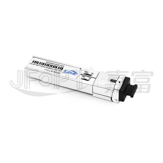
产品型号
|
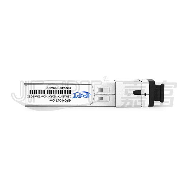
JFTSM-SFP-GPON-C++2.5/1.25-1413-20-SCS
|
工厂品牌
|
JFOPT嘉富
|
|
封装形式
|
SFP
|
光口类型
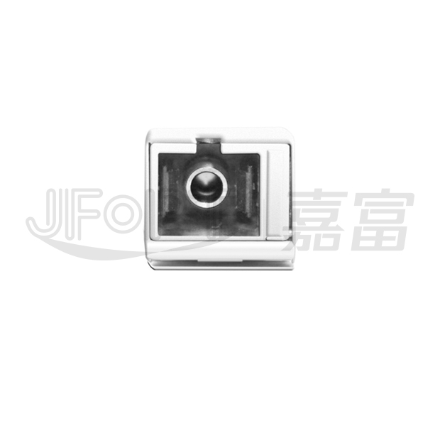
|
SC
|
|
最高总速率
|
2.5/1.25Gbps
|
每通道速率
|
|
|
最大传输距离
|
20km
|
||
|
工作波长
|
1490/1310nm
|
工作电压
|
3.3V
|
|
光纤型号
|
SMF
|
纤芯尺寸
|
9/125
|
|
发射器类型
|
|
接收器类型
|
|
|
发射功率
|
|
接收灵敏度
|
|
|
数字诊断
|
YES
|
接收过载
|
|
|
支持协议
|
|
||
|
工作温度(商业级)
|
|
储存温度(商业级)
|
|
|
工作温度(工业级)
|
|
储存温度(工业级)
|
|
|
工作温度(扩展级)
|
|
储存温度(扩展级)
|
|
生产线介绍
PRODUCTION LINE INTRODUCTION
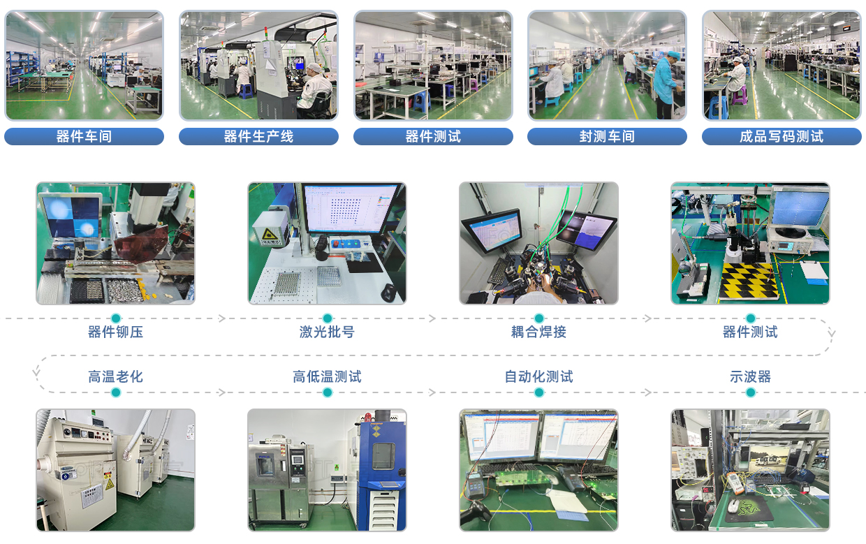
JFOPT嘉富持续投入光模块生产领域,产品覆盖1*9、SFP、10G、25G、100G、200G、400G、800G GPON/EPON/XG/XGSPON OLT等全系列光模块。同时为下游同行提供TOSA、ROSA、BOSA等光器件半成品解决方案。JFOPT嘉富生产线具备日产量一万只光模块、两万只光器件的能力。此外,JFOPT嘉富光模块拥有业界领先的耐高温、抗干扰特性,广泛应用于计算中心、运营商、交通安防、电力设施等行业领域。
产品介绍
PRODUCT PRESENTATION
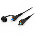
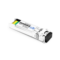
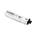
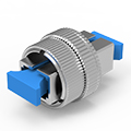
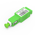
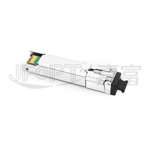
JFOPT GPON OLT C++ 7dBm光模块是一款高端SFP收发器,专为光纤线路终端应用设计,通过单模光纤实现20公里传输距离下的高速非对称数据传输:下行速率2.488Gbps(1490nm波长),上行速率1.244Gbps(1310nm波长)。该模块采用SC/UPC接口,符合增强型GPON C++等级标准,提供7dBm光功率预算,支持单纤双向通信,并遵循SFF-8472协议实现数字诊断监控(DDM)功能以进行实时性能追踪;完全满足ITU-T G.984.2标准及RoHS环保合规要求。
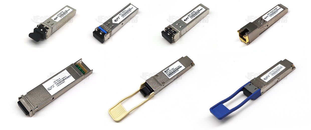
光模块系列产品
TRANSCEIVER SERIES PRODUCTS
生产及检测设备
PRODUCTION & TESTING EQUIPMENT
产品特点
FEATURES
| Single power supply 3.3V | Small form-factor pluggable (SFP) | ||||||||
| Digital diagnostic monitor compatible with SFF-8472 | SC receptacle optical connector | ||||||||
| Integrated WDM filter for dual wavelength operate at 1490 Tx/1310nm Rx | 1490nm DFB continuos-mode transmitter | ||||||||
| 1310nm burst-mode APD-TIA receiver | LVTTL transmitter disable input and transmitter fault output | ||||||||
| hot pluggable capability | LVPECL compatible data input/output interface |
应用范围
APPLICATION
Gigabit Ethernet Passive Optical Networks (GPON CLASS C++) –OLT side |
符合标准
STANDARD COMPLIANCE

订购信息
ORDER INFORMATION
| Part No. | Data Rate | Tx Power | Connector Type | Fiber Type | Distance | Temp. | DDMI | ||
| JFTSM-SFP-GPON-C++2.5/1.25-1413-20-SCS | 2.5/1.25G | 4.5~10dBm | SC | Single Fiber | 20km | 0~+70°C | YES | ||
绝对最大额定值
ABSOLUTE MAXIMUM RATINGS
| Parameter | Symbol | Min. | Max. | Unit | |||||
| Storage Temperature | TS | -40 | +85 | ℃ | |||||
| Operating Temperature | Top | 0 | +70 | ℃ | |||||
| Supply Voltage | VCC | -0.5 | +3.6 | V | |||||
| Power Supply Current | ICC | - | 400 | mA | |||||
| Voltage at Any Input Pin | VIN | 0 | Vcc | V | |||||
推荐操作条件
RECOMMENDED OPERATING CONDITIONS
| Parameter | Symbol | Min. | Typical | Max. | Unit | ||||
| Operating Temperature | Top | 0 | - | +70 | ℃ | ||||
| Supply Voltage | VCC | 3.1 | 3.3 | 3.5 | V | ||||
| Tx Data Rate | - | - | 2488 | - | Mb/s | ||||
| Rx Data Rate | - | - | 1244 | - | Mb/s | ||||
光学和电气特性
OPTICAL & ELECTRICAL CHARACTERISTICS
| Parameter | Symbol | Min. | Typ. | Max. | Unit | ||||
Transmitter(T=0 to +70℃, VCC =3.1~3.5V) |
|||||||||
| Central Wavelength | λC | 1480 | 1490 | 1500 | nm | ||||
| Spectral Width | Δλ | - | - | 1 | nm | ||||
| Side Mode Suppression Ratio | SMSR | 30 | - | - | dB | ||||
| Output Power | Po | 4.5 | - | 10 | dBm | ||||
| Extinction Ratio | ER | 8.2 | - | - | dB | ||||
| Output Power at Transmit Off | - | - | - | -40 | dBm | ||||
| Differential Input Voltage | VIH- VIL | 200 | - | 1600 | mV | ||||
| TX Disable Input Voltage Low | TX_DISABLEL | 0 | - | 0.8 | V | ||||
| TX Disable Input Voltage High | TX_DISABLEH | 2.0 | - | Vcc | V | ||||
| TX Fault Output Voltage Low | TX_FAULTL | 0 | - | 0.8 | V | ||||
| TX Fault Output Voltage High | TX_FAULTH | 2.0 | - | VCC+0.3 | V | ||||
| Eye Diagram | Compliance with ITU-T G.984.2 | ||||||||
Receiver(T=0 to +70℃, VCC =3.1~3.5V) |
|||||||||
| Wavelength Range | λ | 1260 | - | 1360 | nm | ||||
| MIN. Input Power (Sensitivity) | PMIN | - | - | -31 | dBm | ||||
| MAX. Input Power (Saturation) | PMAX | -12 | - | - | dBm | ||||
| Signal Detect-Asserted | PA | - | - | -30 | dBm | ||||
| Signal Detect-Deasserted | PD | -45 | - | - | dBm | ||||
| Signal Detect Hysteresis | PHYS | 0.5 | - | 6 | dB | ||||
| Return Loss | ORL | 12 | - | - | dB | ||||
| RX Loss of Signal Output Voltage Low | RX_LOSL | 0 | - | 0.8 | V | ||||
| RX Loss of Signal Output Voltage High | RX_LOSH | 2.0 | - | VCC+0.3 | V | ||||
| LOS Assert Time | TAssert | - | - | 100 | ns | ||||
| LOS De-assert Time | TDeassert | - | - | 12.8 | ns | ||||
数字RSSI定时规范
DIGITAL RSSI TIMING SPECIFICATION
| Parameter |
Minimum
|
Typical | Maximum | Unit | Notes | ||||
| RSSI Trigger Delay | 25 | - | - | ns | - | ||||
| RSSI Sampling Time | 300 | - | - | ns | - | ||||
| Internal I2C Delay | - | - | 500 | us | - | ||||
| Receiver Power DDM(RSSI)Error | - | - | +/-3 | dB | - | ||||
| a) RSSI_ACQ input signal rising edge will trigger RSSI sampling, and falling edge will trigger internal digital RSSI information written to I2C. It is recommended that host shall not trigger RSSI_ACQ input again until RSSI data is valid inI2C from previous RSSI trigger. b) RSSI DDM working range is between -8 to -28dBm. RSSI DDM accuracy is better than +/-3dB for input power level between -10 to -28dBm, the accuracy reduces to +/-5dBm to -10 dBm. If the data pattern is at least 2^7-1 or longer, a minimum average of 8 times is strongly recommended to maintain the RSSI reading accuracy. |
|||||||||
EEPROM串行ID存储器内容(A0h)
EEPROM SERIAL ID MEMORY CONTENTS (A0H)
| Address | Size (Bytes) |
Name of Field | Hex | Description of Field | |||||
| 0 | 1 | Identifier | 03 | SFP | |||||
| 1 | 1 | Ext. Identifier | 04 | MOD4 | |||||
| 2 | 1 | Connector | 01 | SC | |||||
| 3—10 | 8 | Transceiver | 00 00 00 00 00 00 00 00 | Transceiver Code Field,not applicable | |||||
| 11 | 1 | Encoding | 03 | NRZ encoding | |||||
| 12 | 1 | BR, nominal | 19 | 2488.32Mbps | |||||
| 13 | 1 | Reserved | 00 | Reserved | |||||
| 14 | 1 | Length(9um)-km | 14 | 20(Units of km) | |||||
| 15 | 1 | Length (9um) | C8 | 200(Units of 100 m) | |||||
| 16 | 1 | Length (50um) | 00 | Not Support MMF | |||||
| 17 | 1 | Length (62.5um) | 00 | Not Support MMF | |||||
| 18 | 1 | Length (copper) | 00 | Not Support Copper | |||||
| 19 | 1 | Reserved | 00 | - | |||||
| 20—35 | 16 | Vendor name | XXXXX | “ODI” | |||||
| 36 | 1 | Reserved | 00 | - | |||||
| 37—39 | 3 | Vendor OUI | 000000 | - | |||||
| 40—55 | 16 | Vendor PN | XXXXX | “PART NUMBER ” (ASCⅡ) | |||||
| 56—59 | 4 | Vendor rev | xxxx xxxx | ASCⅡ (“31 2E 31 20” means 1. 1 revision) | |||||
| 60-61 | 2 | Wavelength | 05 D2 | 1490nm Laser wavelength | |||||
| 62 | 1 | Reserved | 00 | - | |||||
| 63 | 1 | CC BASE | xx | Checksum of bytes 0 - 62 | |||||
| 64—65 | 2 | Options | 00 1A | LOS, TX_FAULT and TX_DISABLE | |||||
| 66 | 1 | BR, max | 00 | - | |||||
| 67 | 1 | BR, min | 00 | - | |||||
| 68—83 | 16 | Vendor SN | xxxx xxxx xxxx xxxx xxxx xxxx xxxx xxxx |
SN :xxxxxxxxx (ASCⅡ) | |||||
| 84—91 | 8 | Vendor date code | xxxx xxxx xxxx 20 20 | Year (2 bytes), Month (2 bytes), Day (2 bytes) (ASCⅡ) |
|||||
| 92 | 1 | Diagnostic type | 58 | Externally Calibrated | |||||
| 93 | 1 | Enhanced option | B0 | Diagnostic(Optional Alarm/warning flags) Soft TX_FAULT monitoring implemented Soft RX_LOS monitoring implemented |
|||||
| 94 | 1 | SFF-8472 | 01 | Includes functionality described in Rev 9. 4 SFF-8472 |
|||||
| 95 | 1 | CC_EXT | xx | Checksum of bytes 64 - 94 | |||||
| 96—127 | 32 | Vendor specific | - | Vendor Specific EEPROM | |||||
| 128-255 | 128 | Reserved | - | Reserved for future use. | |||||
| Note: 1.The“ xx” byte should be filled in according to practical case. 2. Note that, A0H is readable and writeable , A2H is readable and write-protected. |
|||||||||
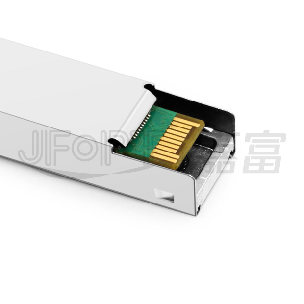
引脚分配
PINS ASSIGNMENT
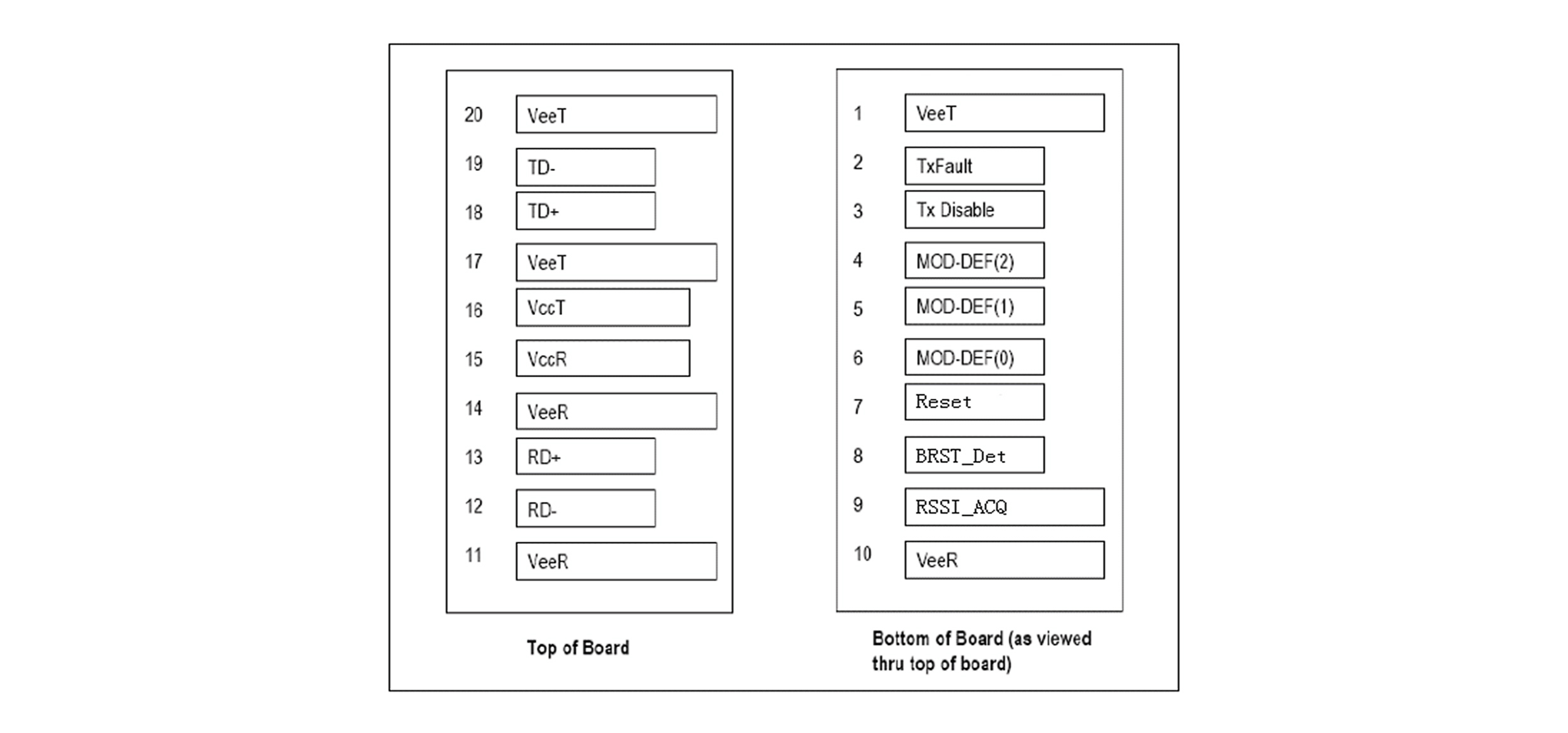
引脚功能定义
PINS FUNCTION DEFINITION
| Pin No. | Name | Function | Plug Seq. | Notes | |||||
| 1 | VeeT | Tx Ground | 1 | - | |||||
| 2 | TX Fault | Transmitter Fault Indication,LVTTL Output Active High | 3 | Note 1 | |||||
| 3 | TX Disable | Transmitter Disable,LVTTL input. | 3 | Note 2 | |||||
| 4 | MOD-DEF2 | 2-Write Serial Data I/O Pin. | 3 | Note 3 | |||||
| 5 | MOD-DEF1 | 2-Write Serial Data I/O Pin. | 3 | Note 3 | |||||
| 6 | MOD-DEF0 | Internally Grounded | 3 | Note 3 | |||||
| 7 | Reset | CMOS input.Assert “Reset” high at the end of previous burst,2 byte in duration | 3 | - | |||||
| 8 | BRST_Det | LVTTL output.BRST_Det assert low when module receives “reset”signal, assert high when incoming burst is present. |
3 | Note 4 | |||||
| 9 | RSSI_ACQ | RSSI acquire/hold LVTTL input. Digital RSSI output through I2C | 1 | - | |||||
| 10 | VeeR | Receiver Ground | 1 | - | |||||
| 11 | VeeR | Receiver Ground | 1 | - | |||||
| 12 | RD- | Inv. Received Data Out | 3 | Note 5 | |||||
| 13 | RD+ | Received Data Out | 3 | Note 5 | |||||
| 14 | VeeR | Receiver Ground | 1 | - | |||||
| 15 | VccR | Receiver Power | 2 | - | |||||
| 16 | VccT | Transmitter Power | 2 | - | |||||
| 17 | VeeT | Transmitter Ground | 1 | - | |||||
| 18 | TD+ | Transmit Data In | 3 | Note 6 | |||||
| 19 | TD- | Inv Transmit Data In | 3 | Note 6 | |||||
| 20 | VeeT | Transmitter Ground | 1 | - | |||||
| Notes: 1. TX Fault is an open collector output, which should be pulled up with a 4.7K~10KΩ resistor on the host board to a voltage between 2.0V and Vcc+0.3V. Logic 0 indicates normal operation; logic 1 indicates a laser fault of some kind. In the low state, the output will be pulled to less than 0.8V. 2. TX Disable is an input that is used to shut down the transmitter optical output. It is pulled up within the module with a 4.7K~10KΩ resistor. Its states are: Low (0~0.8V): Transmitter on (>0.8V, <2.0V): Undefined High (2.0~3.465V): Transmitter Disabled Open:Transmitter Disabled. 3. MOD-DEF 0,1,2 are the module definition pins. They should be pulled up with a 4.7K~10KΩ resistor on the host board. The pull-up voltage shall be VccT or VccR. MOD-DEF 0 is grounded by the module to indicate that the module is present. MOD-DEF 1 isthe clock line of two wire serial interface for serial ID. MOD-DEF 2 isthe data line of two wire serial interface for serial ID. 4. LOS is an open collector output, which should be pulled up with a 4.7K~10KΩ resistor on the host board to a voltage between 2.0V and Vcc+0.3V. Logic 0 indicates normal operation; logic 1 indicates loss of signal. In the low state, the output will be pulled to less than 0.8V. 5. These are the differential receiver outputs. They are AC coupled 100Ω differential lines which should be terminated with 100Ω (differential) atthe user SERDES. 6. These are the differential transmitter inputs. They are AC-coupled, differential lines with 100Ω differential termination inside the module. |
|||||||||
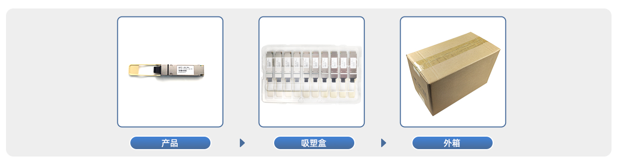
产品包装
PRODUCT PACKAGING
产品认证
PRODUCT CERTIFICATION

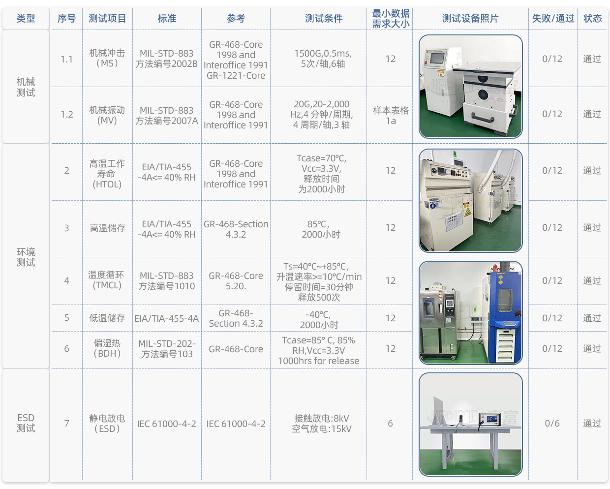
质量优势
QUALITY ADVANTAGE
兼容品牌
COMPATIBLE BRANDS


 Wendy
Wendy Sophie
 Jeanne