


| 产品型号 | JFTSM-SFP+16-CW1416-10/40-LCD | 工厂品牌 | JFOPT嘉富 |
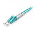
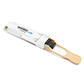
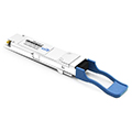
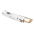
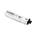
| 封装形式 | SFP+ | 光口类型 | LC Duplex |
| 最高总速率 | 14.025Gbps | 每通道速率 | 14.025Gbps |
| 最大传输距离 | 40km | 功率预算 | 14dB |
| 工作波长 | 1470nm to 1610nm | 工作电压 | 3.3V |
| 光纤型号 | SMF | 纤芯尺寸 | 9/125 |
| 发射器类型 | CWDM EML |
接收器类型 | IDP |
| 发射功率 | 0~4dBm | 接收灵敏度 | -14dBm |
| 数字诊断 | YES | 接收过载 | 0dBm |
| 功耗 | <1.8W | 支持协议 | SFF-8431 SFF-8432 SFF-8472 |
| 工作温度(商业级) | 0℃~+70℃ | 储存温度(商业级) | -40℃~+85℃ |
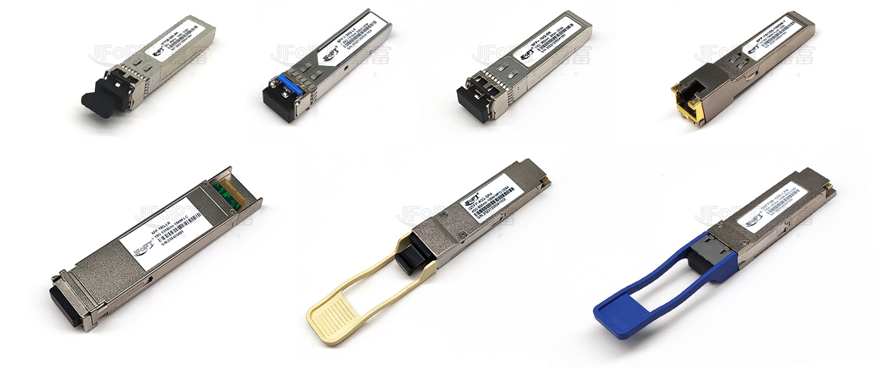
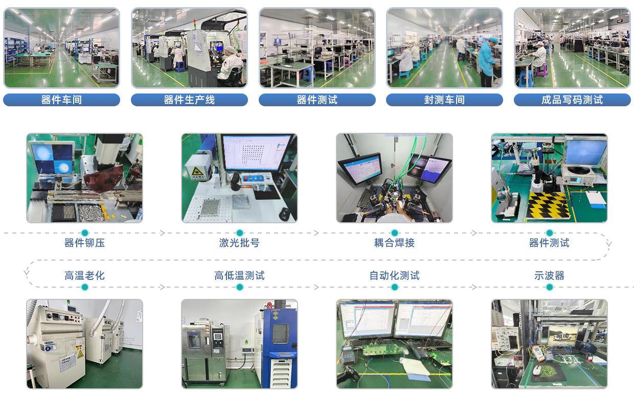
JFOPT嘉富持续投入光模块生产领域,产品覆盖1*9、SFP、10G、25G、100G、200G、400G、800G GPON/EPON/XG/XGSPON OLT等全系列光模块。同时为下游同行提供TOSA、ROSA、BOSA等光器件半成品解决方案。JFOPT嘉富生产线具备日产量一万只光模块、两万只光器件的能力。此外,JFOPT嘉富光模块拥有业界领先的耐高温、抗干扰特性,广泛应用于计算中心、运营商、交通安防、电力设施等行业领域。
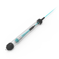
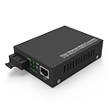
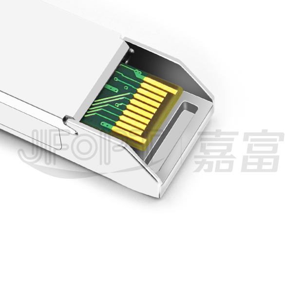
JFOPT SFP+ 16G CWDM(1470-1610nm)10/40km LC DX系列是一款紧凑型可插拔单模光模块,专为串行光数据通信设计(支持16倍速/8倍速/4倍速光纤通道应用);该模块针对单模光纤优化,在1470nm至1610nm标称CWDM波长范围内工作(波长间隔20nm),提供14dB光链路预算保证。配备SFP+ 20-pin连接器,支持热插拔功能;发射端采用符合IEC-60825标准1类激光安全的CWDM电吸收调制激光器(EML),接收端则使用PIN探测器与限幅后置放大器IC实现可靠信号接收。该系列模块完全兼容SFP+多源协议(MSA)规范SFF-8431。
| Operating data rate up to 14.025Gbps | 8-Wavelengths CWDM EML transmitter from 1470nm to 1610nm, with step 20nm | ||||||||
| 14dB power budget | Single 3.3V power supply and TTL logic interface | ||||||||
| Duplex LC connector interface | Hot pluggable | ||||||||
| Power dissipation < 1.8W | Operating case temperature Standard: 0℃~+70℃ |
| Multi-rate 16x / 8x / 4x fibre channel | Other optical links |

| Part No. | Data rate | Laser | Fiber type | Power budget | Optical interface | Temp. | DDMI | ||
| JFTSM-SFP+16-CW1416-10/40-LCD | 14.025 Gbps | CWDM EML | SMF | 14dB | LC | Standard | YES | ||
| Parameter | Symbol | Min. | Max. | Unit | |||||
| Storage temperature | Ts | -45 | +85 | °C | |||||
| Supply voltage | Vcc | -0.5 | 3.6 | V | |||||
| Input voltage | Vin | -0.5 | Vcc | V | |||||
*Note:Exceeding any one of these values may destroy the device permanently. |
|||||||||
| Band | Nomenclature | Wavelength(nm) | |||||||
| Min. | Typ. | Max. | |||||||
| S-band Short Wavelength | K | 1464 | 1470 | 1477.5 | |||||
| L | 1484 | 1490 | 1497.5 | ||||||
| M | 1504 | 1510 | 1517.5 | ||||||
| N | 1524 | 1530 | 1537.5 | ||||||
| C-band Conventional | O | 1544 | 1550 | 1557.5 | |||||
|
L-band
Long Wavelength
|
P | 1564 | 1570 | 1577.5 | |||||
| Q | 1584 | 1590 | 1597.5 | ||||||
| R | 1604 | 1610 | 1617.5 | ||||||
| *8 Wavelengths from 1470nm to 1610nm, each step 20nm. |
|||||||||
| Parameter | Symbol | Min. | Typical | Max. | Units | ||||
| Operating case temperature | TC | 0 | - | +70 | °C | ||||
| Power supply voltage | Vcc | 3.15 | 3.3 | 3.45 | V | ||||
| Power supply current | Icc | - | 430 | 545 | mA | ||||
| Surge current | ISurge | - | - | +30 | mA | ||||
| Baud rate | JFTSM-SFP+16-CW1416-10/40-LCD | 4.25 | 14.025 | - | Gbps | ||||
| Parameter | Symbol | Min. | Typ. | Max | Unit | Notes | |||
Transmitter |
|||||||||
| CML inputs(Differential) | Vin | 250 | - | 1000 | mVpp | AC coupled inputs | |||
| Input impedance (Differential) | Zin | 85 | 100 | 115 | ohms | Rin > 100 kohms @ DC | |||
| Differential input S-parameter | SDD11 | - | - | -10 | dB | - | |||
| Differential to common mode conversion | SCD11 | - | - | -10 | dB | - | |||
| Tx_DISABLE input voltage - high | - | 2 | - | 3.45 | V | - | |||
| Tx_DISABLE input voltage - low | - | 0 | - | 0.8 | V | - | |||
| Tx_FAULT output voltage - high | - | 2 | - | Vcc+0.3 | V | Io = 400µA; Host Vcc | |||
| Tx_FAULT output voltage - low | - | 0 | - | 0.5 | V | Io = -4.0mA | |||
Receiver |
|||||||||
| CML outputs (Differential) | Vout | 350 | - | 700 | mVpp | AC coupled outputs | |||
| Output AC common mode voltage | 0 | 15.0 | mV | RMS | |||||
| Output impedance (Differential) | Zout | 85 | 100 | 115 | ohm | - | |||
| Differential output S-parameter | SD22 | - | - | -10 | dB | - | |||
| Rx_LOS output voltage - high | - | 2 | - | Vcc+0.3 | V | lo = 400µA; host Vcc | |||
| Rx_LOS output voltage - low | - | 0 |
-
|
0.8
|
V | lo = -4.0mA | |||
| MOD_DEF ( 0:2 ) | VoH | 2.5 | - | - | V | With serial ID | |||
| VoL | 0 | - | 0.5 | V | |||||
| Parameter | Symbol | Min. | Typical | Max. | Unit | ||||
| Power budget | - | - | 14 | - | dB | ||||
| Data rate | - | 4.25 | 14.025 | - | Gbps | ||||
Transmitter |
|||||||||
| Optical wavelength | λ | λc–6 | λc | λc+7.5 | nm | ||||
| -20dB spectrum width | Δλ | - | - | 1 | nm | ||||
| Side mode suppression ratio | SMSR | 30 | - | - | dB | ||||
| Average output power | Pout | 0 | - | +4 | dBm | ||||
| Extinction ratio | ER | 8.2 | - | - | dB | ||||
| Average power of OFF transmitter | POFF | - | - | -30 | dBm | ||||
| Transmitter dispersion penalty | TDP | - | - | 2.5 | dB | ||||
| TX disable assert time | t_off | - | - | 10 | us | ||||
| TX_DISABLE negate time | t_on | - | - | 1 | ms | ||||
| TX_BISABLE time to start reset | t_reset | 10 | - | - | us | ||||
| Time to initialize, include reset of TX_FAULT | t_init | - | - | 300 | ms | ||||
| TX_FAULT from fault to assertion | t_fault | - | - | 100 | us | ||||
| Total jitter | TJ | - | - | 0.28 | UI(p-p) | ||||
| Data dependant jitter | DDJ | - | - | 0.1 | UI(p-p) | ||||
| Uncorrelated jitter | UJ | - | - | 0.023 | RMS | ||||
Receiver |
|||||||||
| Centre wavelength | λ | 1260 | - | 1620 | nm | ||||
| Sensitivity | Pmin | - | - | -14 | dBm | ||||
| Receiver overload | Pmax | 0 | - | - | dBm | ||||
| Optical return loss | ORL | - | - | -12 | dB | ||||
| LOS de-assert | LOSD | - | - | -16 | dBm | ||||
| LOS assert | LOSA | -26 | - | - | dBm | ||||
| LOS | High | - | 2.0 | - | VCC+0.3 | V | |||
| Low | - | 0 | - | 0.8 | |||||
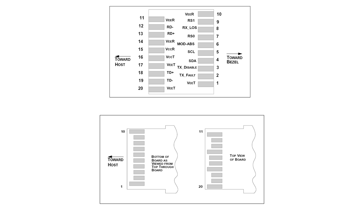
| Pin Num. | Name | Function | Plug Seq. | Notes | |||||
| 1 | VeeT | Transmitter ground | 1 | Note 5 | |||||
| 2 | TX fault | Transmitter fault indication | 3 | Note 1 | |||||
| 3 | TX disable | Transmitter disable | 3 | Note 2, module disables on high or open | |||||
| 4 | SDA | Module definition 2 | 3 | 2-Wire serial interface data line. | |||||
| 5 | SCL | Module definition 1 | 3 | 2-Wire serial Interface clock. | |||||
| 6 | MOD_ABS | Module definition 0 | 3 | Note 3 | |||||
| 7 | RS0 | RX rate select(LVTTL). | 3 | Rate select 0, optionally controls SFP+ module receiver. This pin is pulled low to VeeT with a>30K resistor. | |||||
| 8 | LOS | Loss of signal | 3 | Note 4 | |||||
| 9 | RS1 | TX rate select(LVTTL). | 1 | Rate select 1, optionally controls SFP+ module transmitter. This pin is pulled low to VeeT with a >30K resistor. | |||||
| 10 | VeeR | Receiver ground | 1 | Note 5 | |||||
| 11 | VeeR | Receiver ground | 1 | Note 5 | |||||
| 12 | RD- | Inv. received data out | 3 | Note 6 | |||||
| 13 | RD+ | Received data out | 3 | Note 7 | |||||
| 14 | VeeR | Receiver ground | 1 | Note 5 | |||||
| 15 | VccR | Receiver power | 2 | 3.3V ± 5%, Note 7 | |||||
| 16 | VccT | Transmitter power | 2 | 3.3V ± 5%, Note 7 | |||||
| 17 | VeeT | Transmitter ground | 1 | Note 5 | |||||
| 18 | TD+ | Transmit data in | 3 | Note 8 | |||||
| 19 | TD- | Inv. transmit data in | 3 | Note 8 | |||||
| 20 | VeeT | Transmitter ground | 1 | Note 5 | |||||
Notes:
1) TX Fault is an open collector/drain output, which should be pulled up with a 4.7K – 10KΩ resistor on the host board. Pull up voltage between 2.0V and VccT/R+0.3V. When high, output indicates a laser fault of some kind. Low indicates normal operation. In the low state, the output will be pulled to < 0.8V.
2) TX disable is an input that is used to shut down the transmitter optical output. It is pulled up within the module with a 4.7K – 10 KΩ resistor. Its states are:
Low (0 – 0.8V): Transmitter on
(>0.8, < 2.0V): Undefined
High(2.0 – 3.465V): Transmitter Disabled
Open: Transmitter Disabled
3) Module Absent, connected to VeeT or VeeR in the module.
4) LOS (Loss of Signal) is an open collector/drain output, which should be pulled up with a 4.7K – 10KΩ resistor. Pull up voltage between 2.0V and VccT/R+0.3V. When high, this output indicates the received optical power is below the worst-case receiver sensitivity (as defined by the standard in use). Low indicates normal operation. In the low state, the output will be pulled to < 0.8V.
5) The module signal ground contacts, VeeR and VeeT, should be isolated from the module case.
6) RD-/+: These are the differential receiver outputs. They are AC coupled 100Ω differential lines which should be terminated with 100Ω (differential) at the user SERDES. The AC coupling is done inside the module and is thus not required on the host board. The voltage swing on these lines will be between 350 and 700 mV differential (175 –350 mV single ended) when properly terminated.
7) VccR and VccT are the receiver and transmitter power supplies. They are defined as 3.3V ±5% at the SFP+ connector pin. Maximum supply current is 430mA. Recommended host board power supply filtering is shown below. Inductors with DC resistance of less than 1 ohm should be used in order to maintain the required voltage at the SFP+ input pin with 3.3V supply voltage. When the recommended supply-filtering network is used, hot plugging of the SFP+ transceiver module will result in an inrush current of no more than 30mA greater than the steady state value. VccR and VccT may be internally connected within the SFP+ transceiver module.
8) TD-/+: These are the differential transmitter inputs. They are AC-coupled, differential lines with 100Ω differential termination inside the module. The AC coupling is done inside the module and is thus not required on the host board. The inputs will accept differential swings of 150 – 1200 mV (75 – 600mV single-ended).


 Wendy
Wendy Sophie
 Jeanne