


|
产品型号
|
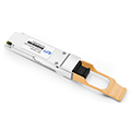
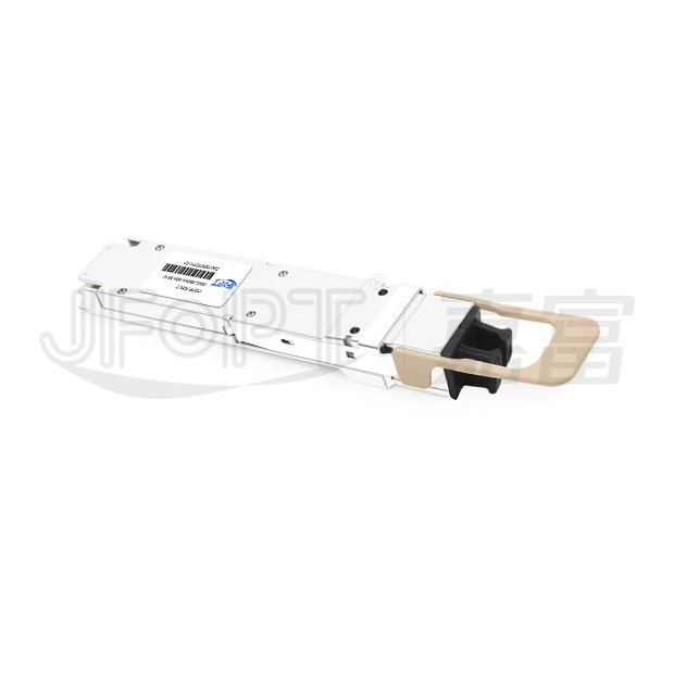
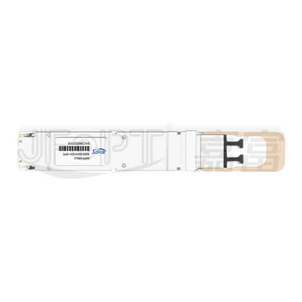
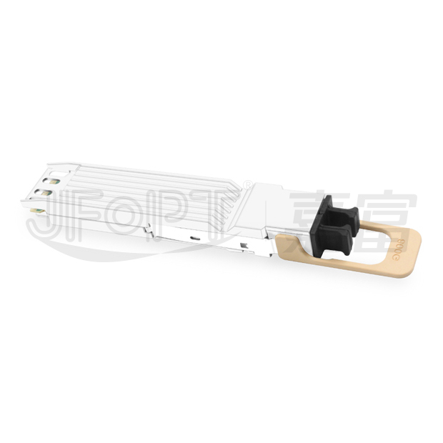
JFTSM-OSFP-800(1x100G)-850-005-(SR8)-MPO16/2MPO8/12
|
工厂品牌
|
JFOPT嘉富
|
|
封装形式
|
OSFP
|
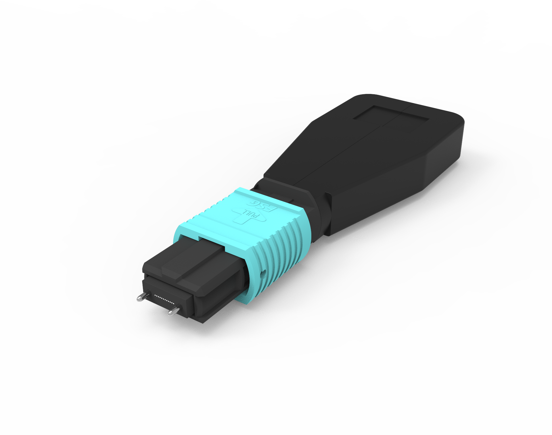
光口类型
|
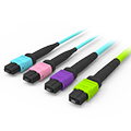
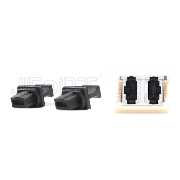
MPO-16 APC
2xMTP-12 APC
|
|
最高总速率
|
800Gbps
|
每通道速率
|
106.25 Gb/s
|
|
OM3最大传输距离
|
30m
|
OM4最大传输距离
|
50m
|
|
工作波长
|
850nm
|
工作电压
|
3.3V
|
|
光纤型号
|
MMF
|
纤芯尺寸
|
50/125
|
|
发射器类型
|
VCSEL
|
接收器类型
|
PIN
|
|
发射功率
|
-4.5~4.0dBm
|
接收灵敏度
|
-6.4dBm
|
|
数字诊断(DOM)
|
YES
|
接收过载
|
4dBm
|
|
功耗
|
<12W
|
支持协议
|
800G BASE-SR8 Ethernet
|
|
工作温度(商业级)
|
0℃~+70℃
|
储存温度(商业级)
|
-40℃~+85℃
|
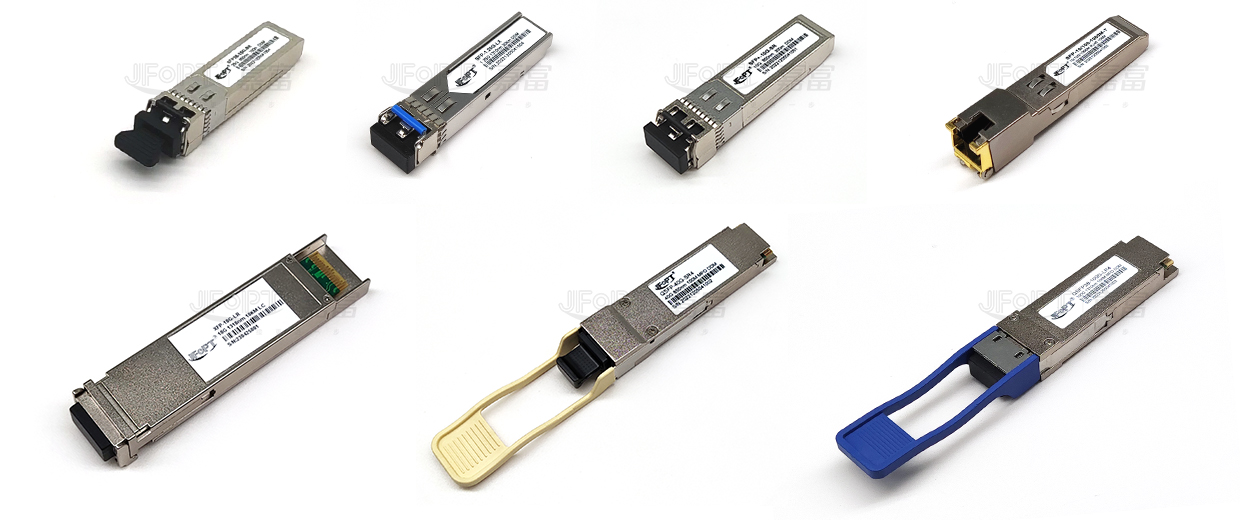
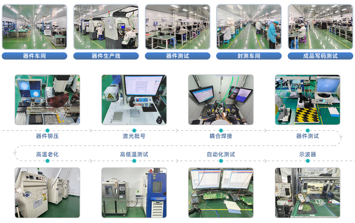
JFOPT嘉富持续投入光模块生产领域,产品覆盖1*9、SFP、10G、25G、100G、200G、400G、800G GPON/EPON/XG/XGSPON OLT等全系列光模块。同时为下游同行提供TOSA、ROSA、BOSA等光器件半成品解决方案。JFOPT嘉富生产线具备日产量一万只光模块、两万只光器件的能力。此外,JFOPT嘉富光模块拥有业界领先的耐高温、抗干扰特性,广泛应用于计算中心、运营商、交通安防、电力设施等行业领域。
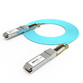
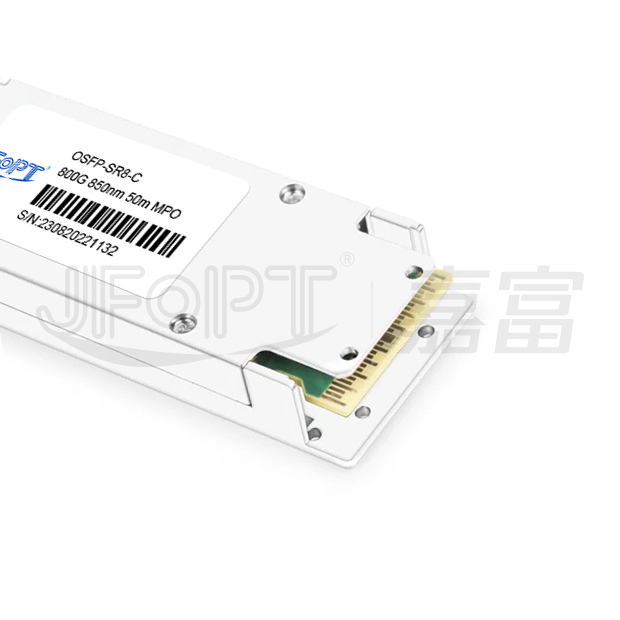
JFOPT OSFP 800G 850nm SR8 MPO16/2MPO8 12光模块是一款先进的8通道可插拔光纤模块,专为800Gbps SR8高速应用设计。该高性能收发器适用于短距离数据通信和互连解决方案,支持每条通道高达106.25Gbps的数据传输速率,通过OM3光纤最远传输30米,OM4光纤最远传输50米,其光接口采用MPO连接器。该模块针对多模光纤系统优化设计,工作波长为850nm,电气接口采用60针边缘型连接器确保稳定可靠的连接,是为满足下一代高速网络需求而设计的尖端解决方案。
| Hot-pluggable OSFP form factor | Data rate 106.25Gb/s PAM4per lane | ||||||||
| 8x106Gbps PAM4 transmitter and PAM4 receiver | 8 channels 850nm VCSEL laser array and 8 channels PIN photo-detector array | ||||||||
| Maximum link length of 30m on OM3 MMF and 50m on OM4 MMF | Digital diagnostics functions are available via the I2C interface | ||||||||
| Single 3.3V power supply and power dissipation<12W | MPO-16APC or 2xMTP-12 APC connector | ||||||||
| Operating case temperature:0℃~+70℃ |
| 800G BASE-SR8 ethernet | ||||||||

| Parameter | Symbol | Min. | Max. | Unit | |||||
| Power supply voltage | VCC | -0.5 | +3.6 | V | |||||
| Storage temperature | TC | -40 | +85 | ℃ | |||||
| Relative humidity | RH | 5 | 85 | % | |||||
These values represent the damage threshold of the module.Stress in excess of any of the individual absolute maximum ratingscan cause immediate catastrophic damage to the module even if all other parameters are within recommended operating conditions.
| Parameter | Symbol | Min | Typical | Max | Unit | ||||
| Power supply voltage | VCC | 3.15 | 3.30 | 3.45 | V | ||||
| Operating case temperature | Tca | 0 | - | 70 | ℃ | ||||
Recommended operating environment specifies parameters for which the electrical and optical characteristics hold unless otherwise noted.
| Parameter | Symbol | Min | Typical | Max | Unit | Notes | |||
| Data rate per lane | DR | - | 106.25 | - | Gbps | - | |||
Transmitter |
|||||||||
| Single ended output voltage tolerance | - | -0.3 | - | 4.0 | V | - | |||
| Common mode voltage tolerance | - | 15 | - | - | mV | - | |||
| Input differential impedance | Rin | - | 100 | - | Ω | - | |||
| Differential input voltage swing | Vin | 300 | - | 1100 | mV | - | |||
| Tx fault | VoL | -0.3 | - | 0.4 | V | At 0.7mA | |||
Receiver |
|||||||||
| Single ended output voltage tolerance | - | -0.3 | - | 4.0 | V | - | |||
| Differential output swing | Vout | 300 | - | 900 | mV | - | |||
| Output differential impedance | Rout | - | 100 | - | Ω | - | |||
The following electrical characteristics are defined over the recommended operating environment unless otherwise specified.
| Parameter | Symbol | Min | Typical | Max | Unit | Notes | |||
Transmitter |
|||||||||
| Center wavelength | λ | 844 | 850 | 863 | nm | - | |||
| RMS spectral width | Pm | - | - | 0.6 | nm | 1 | |||
| Average optical power | Po | -4.5 | - | 4 | dBm | 2 | |||
| Extinction ratio | ER | 2.5 | - | - | dBm | - | |||
| Optical modulation amplitude(OMAouter) (max) |
OMA | 3.5 | dBm | - | |||||
| Optical Modulation Amplitude(OMAouter) (min) max(TECQ,TDECQ)≤1.8dB 1.8 |
-2.6 4.4+max(TECQ,TDECQ) |
- | |||||||
| Transmitter and dispersion eye closure | TDECQ | - | - | 4.4 | dB | - | |||
| Transmitter eye closure | TDEC | - | - | 4.4 | dB | - | |||
| Optical return loss tolerance | ORL | - | - | 12 | dB | - | |||
| Receiver | |||||||||
| Center wavelength | λ | 842 | 850 | 948 | nm | ||||
| Average receive power,each lane | - | -6.4 | - | 4 | dBm | - | |||
| Receive power(OMAouter),each lane | - | - | - | 3.5 | dBm | - | |||
| Receiver sensitivity(OMAouter) Max(TECQ,TDECQ)≤1.8dB 1.8 |
Psens | -4.6 -6.4+TECQ |
dBm | 3 | |||||
| LOS asserted | Lsa | -15 | - | - | dBm | - | |||
| LOS De-asserted | Lda | - | - | -6.6 | dBm | - | |||
| LOS hysteresis | Lh | 0.5 | - | - | dB | - | |||
Note: [1]Trade-offs are available between spectralwidth,center wavelength and minimum OMA. [2]The optical power is launched into MMF. [3]BER=2.4E-4;PRBS31Q@53.125GBd. |
|||||||||
The following optical characteristics are defined over the recommended operating environment unless otherwise specified.
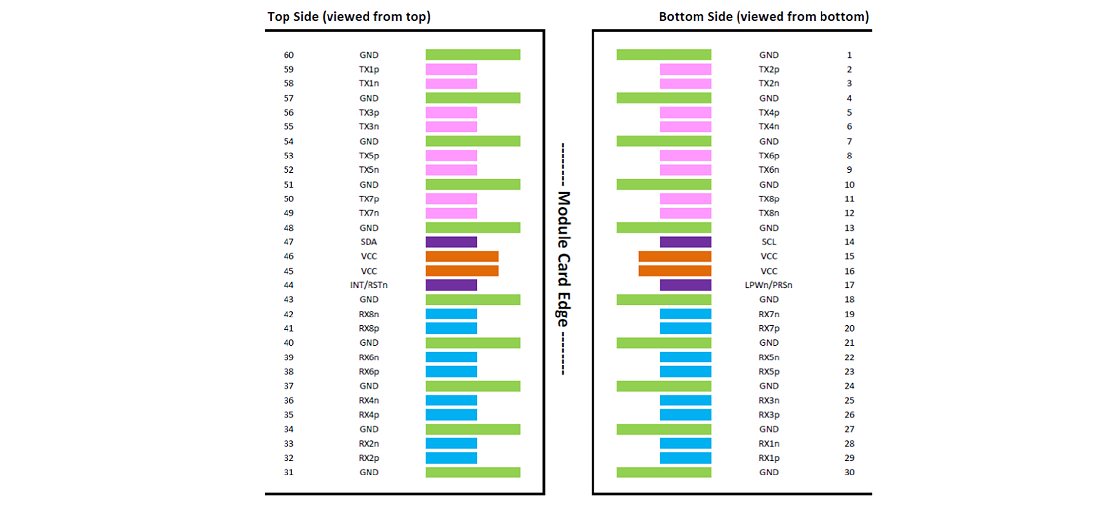
| Pin | Symbol | Name/Description | |||||||
| 1 | GND | Ground | |||||||
| 2 | TX2p | Transmitter data non-inverted | |||||||
| 3 | TX2n | Transmitter data inverted | |||||||
| 4 | GND | Ground | |||||||
| 5 | Tx4p | Transmitter data non-inverted | |||||||
| 6 | TX4n | Transmitter data inverted | |||||||
| 7 | GND | Ground | |||||||
| 8 | TX6p | Transmitter data non-inverted | |||||||
| 9 | TX6n | Transmitter data inverted | |||||||
| 10 | GND | Ground | |||||||
| 11 | TX8p | Transmitter data non-inverted | |||||||
| 12 | TX8n | Transmitter data inverted | |||||||
| 13 | GND | Ground | |||||||
| 14 | SCL | 2-wire Serial interface clock | |||||||
| 15 | VCC | +3.3V Power | |||||||
| 16 | VCC | +3.3V Power | |||||||
| 17 | LPWn/PRSn | Low-power mode/module present | |||||||
| 18 | GND | Ground | |||||||
| 19 | RX7n | Receiver data inverted | |||||||
| 20 | RX7p | Receiver data non-inverted | |||||||
| 21 | GND | Ground | |||||||
| 22 | RX5n | Receiver data inverted | |||||||
| 23 | RX5p | Receiver data non-inverted | |||||||
| 24 | GND | Ground | |||||||
| 25 | RX3n | Receiver data inverted | |||||||
| 26 | RX3p | Receiver data non-inverted | |||||||
| 27 | GND | Ground | |||||||
| 28 | RX1n | Receiver data inverted | |||||||
| 29 | RX1p | Receiver data non-inverted | |||||||
| 30 | GND | Ground | |||||||
| 31 | GND | Ground | |||||||
| 32 | RX2p | Receiver data non-inverted | |||||||
| 33 | RX2n | Receiver data inverted | |||||||
| 34 | GND | Ground | |||||||
| 35 | RX4p | Receiver data non-inverted | |||||||
| 36 | RX4n | Receiver data inverted | |||||||
| 37 | GND | Ground | |||||||
| 38 | RX6p | Receiver data non-inverted | |||||||
| 39 | RX6n | Receiver data inverted | |||||||
| 40 | GND | Ground | |||||||
| 41 | RX8p | Receiver data non-inverted | |||||||
| 42 | RX8n | Receiver data inverted | |||||||
| 43 | GND | Ground | |||||||
| 44 | INT/RSTn | Module interrupt/module reset | |||||||
| 45 | VCC | +3.3V power | |||||||
| 46 | VCC | +3.3V power | |||||||
| 47 | SDA | 2-wire serial interface data | |||||||
| 48 | GND | Ground | |||||||
| 49 | TX7n | Transmitter data inverted | |||||||
| 50 | TX7p | Transmitter data non-inverted | |||||||
| 51 | GND | Ground | |||||||
| 52 | TX5n | Transmitter data inverted | |||||||
| 53 | TX5p | Transmitter data non-inverted | |||||||
| 54 | GND | Ground | |||||||
| 55 | TX3n | Transmitter dataInverted | |||||||
| 56 | TX3p | Transmitter data non-inverted | |||||||
| 57 | GND | Ground | |||||||
| 58 | TX1n | Transmitter data inverted | |||||||
| 59 | TX1p | Transmitter data non-inverted | |||||||
| 60 | GND | Ground | |||||||


 Wendy
Wendy Sophie
 Jeanne