


|
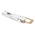
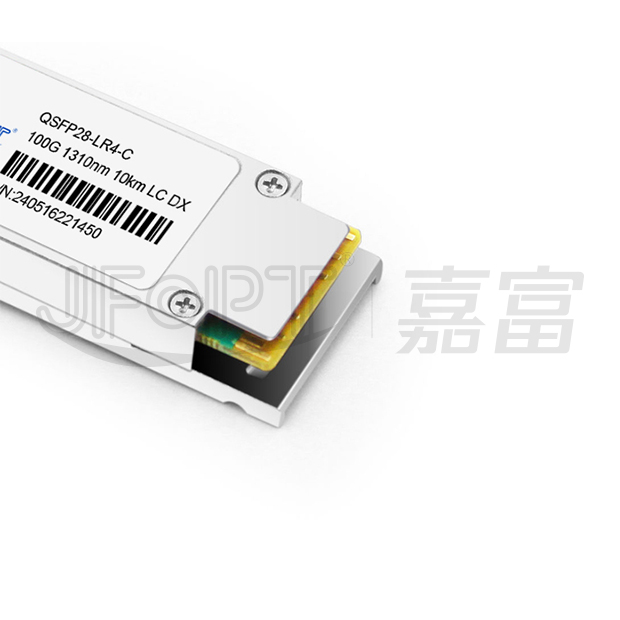
产品型号
|
JFTSM-QSFP28-100-LW-10(LR4)-LCD
|
工厂品牌
|
JFOPT嘉富
|
|
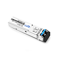
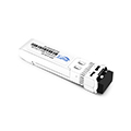
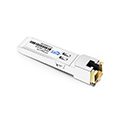
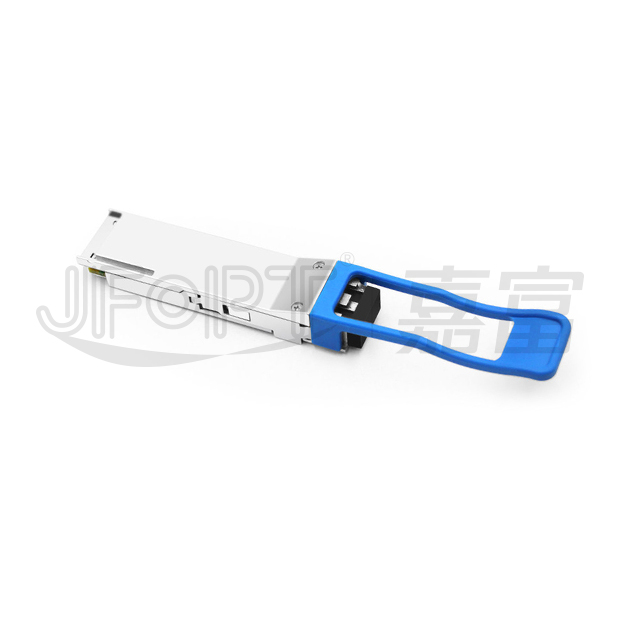
封装形式
|
QSFP28
|
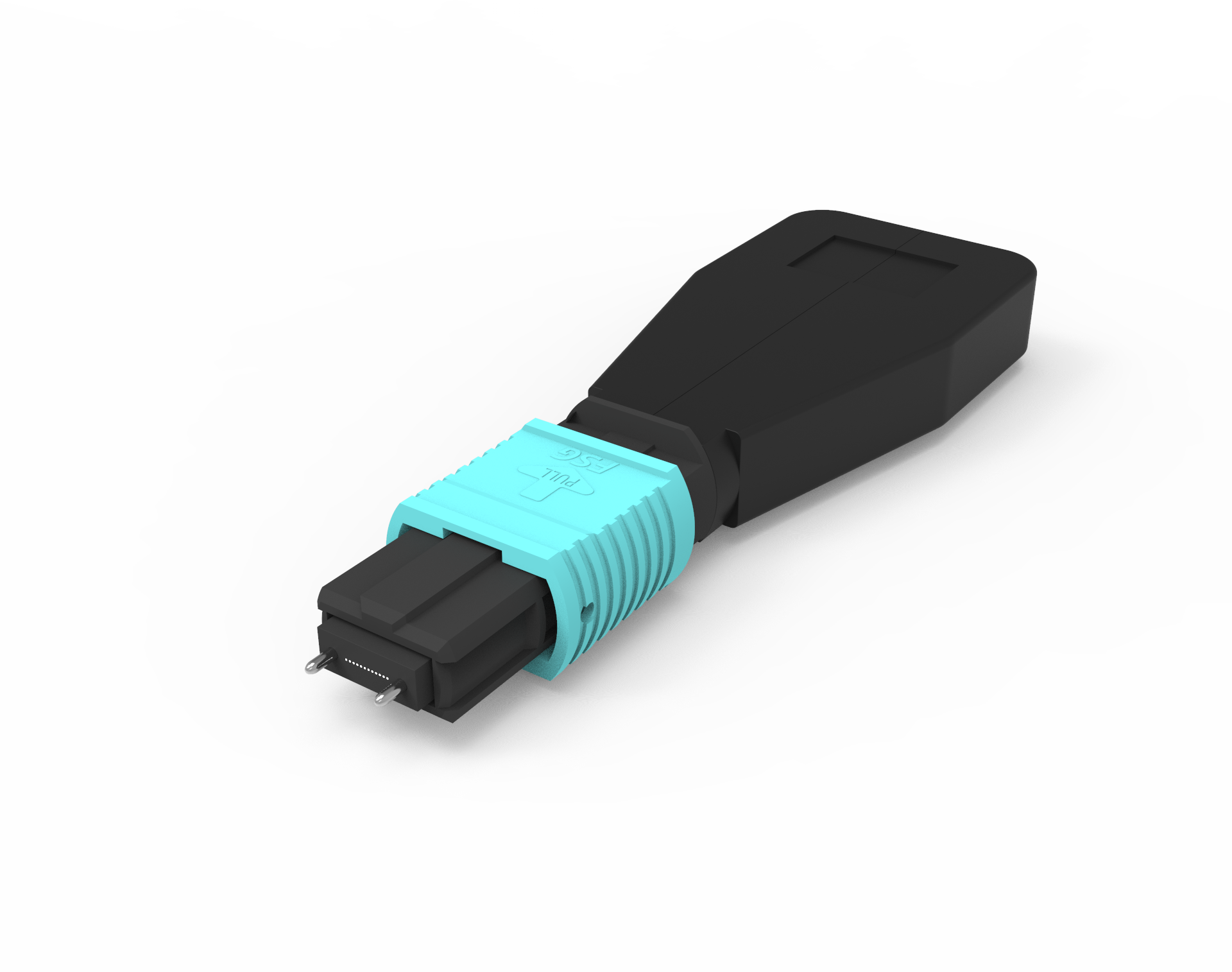
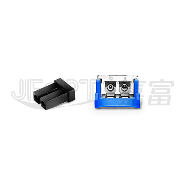
光口类型
|
LC DX
|
|
最高总速率
|
100Gbps
|
每通道速率
|
25.78125Gbps
|
|
最大传输距离
|
10km
|
||
|
工作波长
|
1310nm
|
工作电压
|
3.3V
|
|
光纤型号
|
SMF
|
纤芯尺寸
|
9/125
|
|
发射器类型
|
DFB
|
接收器类型
|
DIN
|
|
发射功率
|
-4.3~4.5dBm
|
接收灵敏度
|
-8.6Bm
|
|
数字诊断(DOM)
|
YES
|
接收过载
|
4.5dBm
|
|
功耗
|
<4W
|
支持协议
|
100GBASE-LR4
100G Ethernet |
|
工作温度(商业级)
|
0℃~+70℃
|
储存温度(商业级)
|
-40℃~+85℃
|
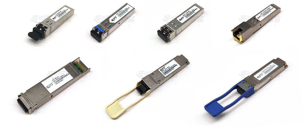
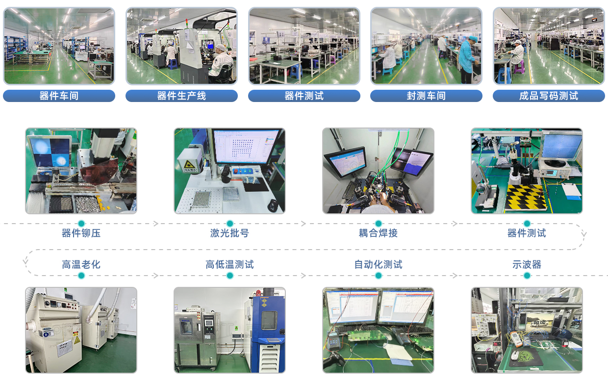
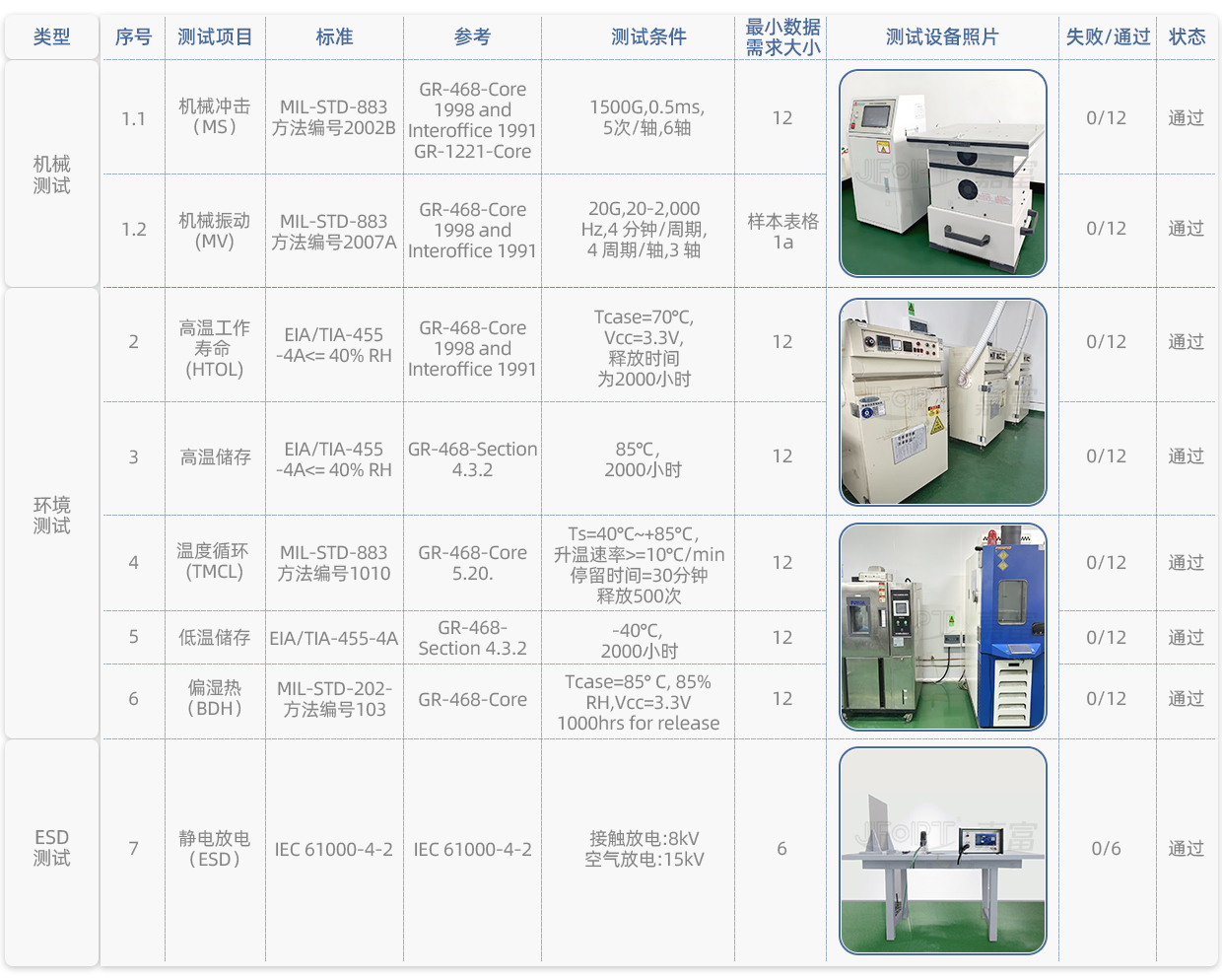
JFOPT嘉富持续投入光模块生产领域,产品覆盖1*9、SFP、10G、25G、100G、200G、400G、800G GPON/EPON/XG/XGSPON OLT等全系列光模块。同时为下游同行提供TOSA、ROSA、BOSA等光器件半成品解决方案。JFOPT嘉富生产线具备日产量一万只光模块、两万只光器件的能力。此外,JFOPT嘉富光模块拥有业界领先的耐高温、抗干扰特性,广泛应用于计算中心、运营商、交通安防、电力设施等行业领域。
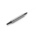
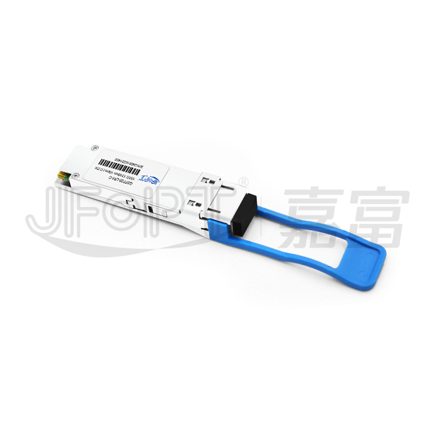
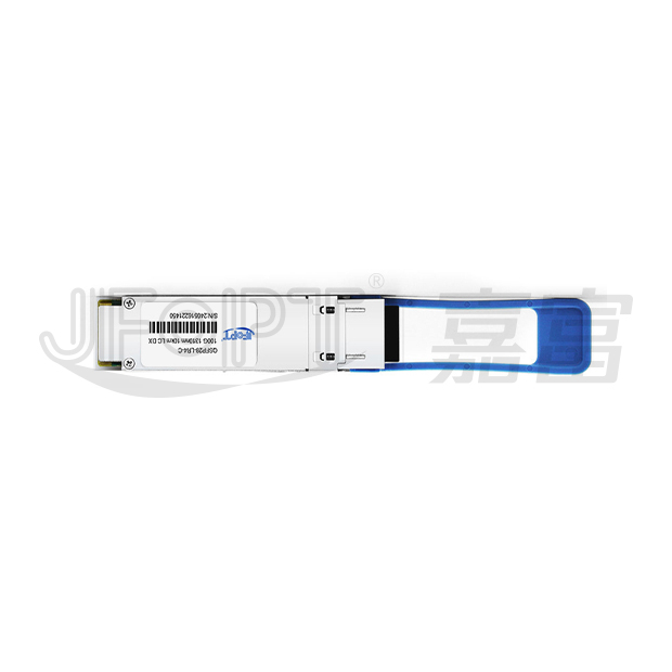
JFOPT QSFP28 100G LAN-WDM 10公里双工LC光模块(符合OTU4 411-9D1F标准)是一款专为光通信应用设计的100Gb/s收发器,严格遵循ITU-T G.959.1、G.709建议书及G.sup39补充协议规范;该模块将四路28Gb/s输入电信号转换为四路局域网波分复用(LAN WDM)光信号,经复用形成单通道100Gb/s光传输,接收端则将100Gb/s光输入解复用为四路LAN WDM光信号并转换为四路输出电信号;其四通道中心波长(1295.56nm/1300.05nm/1304.58nm/1309.14nm)严格符合IEEE 802.3ba定义的LAN-WDM波长栅格,搭载高性能制冷式LAN WDM DFB发射器与高灵敏度PIN接收器确保卓越性能;基于QSFP+多源协议(MSA)设计,具备紧凑型结构、强固型光电接口及数字诊断功能,可在极端温度、高湿及强电磁干扰(EMI)等严苛环境下稳定运行,是高性能应用的理想解决方案。
| Supports 103Gbps | I2C interface with integrated digital diagnostic monitoring | ||||||||
| 4*25Gbps DFB-based LAN-WDM transmitter | PIN and TIA array on the receiver side | ||||||||
| 4*25G electrical interface | Single 3.3V power supply and power dissipation<4W | ||||||||
| Distance up to 10km over SMF | Duplex LC receptacles | ||||||||
| Operatingcase temperature:0℃~+70℃ |
| 100GBASE-LR4 100G ethernet | ||||||||

| Parameter | Symbol | Min. | Max. | Unit | |||||
| Power supply voltage | VCC | -0.5 | +3.6 | V | |||||
| Storage temperature | TC | -40 | +85 | ℃ | |||||
| Relative humidity | RH | 5 | 85 | % | |||||
These values represent the damage threshold of the module.Stress in excess of any of the individual absolute maximum ratingscan cause immediate catastrophic damage to the module even if all other parameters are within recommended operating conditions.
| Parameter | Symbol | Min | Typical | Max | Unit | ||||
| Power supply voltage | VCC | 3.15 | 3.30 | 3.45 | V | ||||
| Operating case temperature | Tca | 0 | - | 70 | ℃ | ||||
| Parameter | Symbol | Min | Typical | Max | Unit | Ref | |||
Transmitter |
|||||||||
| Input differential impedance | Rin | - | 100 | - | Ω | 1 | |||
| Single-ended input voltage tolerance | - | -0.3 | - | 4.0 | V | - | |||
| AC common mode input voltage tolerance | - | 15 | - | - | mV | - | |||
| Differential input voltage | - | 50 | - | - | mV | - | |||
| Differential input voltage swing,per lane | Vin | 190 | - | 1000 | mV | - | |||
Receiver |
|||||||||
| Output differential impedance | Rout | - | 100 | - | Ω | 1 | |||
| Differential output swing,per lane | Vout | 300 | - | 900 | mV | 2 | |||
| AC common mode output voltage tolerance | - | - | - | 7.5 | mV | - | |||
| Single-ended output voltage | - | -0.3 | - | 4.0 | V | - | |||
Notes: [1]AC coupled. [2]Into 100 ohm differentialter mination. |
|||||||||
| Parameter | Symbol | Min | Typical | Max | Unit | Ref. | |||
| Bit rate per lane | DR | 25.78125±100ppm | Gb/s | 1 | |||||
| Data rate variation | - | -100 | - | 100 | ppm | - | |||
| Lane_0 center wavelength | λ0 | 1294.53 | 1295.56 | 1296.59 | nm | - | |||
| Lane_1 center wavelength | λ1 | 1299.02 | 1300.05 | 1301.09 | nm | - | |||
| Lane_2 center wavelength | λ2 | 1303.54 | 1304.58 | 1305.63 | nm | - | |||
| Lane_3 center wavelength | λ3 | 1308.09 | 1309.14 | 1310.19 | nm | - | |||
| Total average output power | Po | - | - | 10.5 | dBm | - | |||
| Average launch power each lane | - | -4.3 | - | 4.5 | dBm | 2,7 | |||
| Optical modulation amplitude (OMA)each lane | OMA | -1.3 | - | 4.5 | dBm | - | |||
| Difference in launch power between any two lanes(OMA) | - | - | - | 5 | dB | - | |||
| Launch power in OMA minus TDP, each lane | OMA-TDP | -2.3 | - | - | dBm | - | |||
| Transmitter and dispersion penalty(TDP),each lane | TDP | - | - | 2.2 | dB | - | |||
| Extinction ratio | ER | 4 | - | - | dB | - | |||
| Side-mode suppression ratio | SMSR | 30 | - | - | dB | - | |||
| Average launch power of OFF transmitter per lane | Poff | - | - | -30 | dBm | - | |||
| Transmitter reflectance | - | - | - | -12 | dB | - | |||
| Optical return loss tolerance | ORL | - | - | 20 | dB | - | |||
| Transmitter eye mask definition{X1,X2,X3,Y1,Y2,Y3} | {0.25,0.4,0.45,0.25,0.28,0.4} | 3 | |||||||
| Parameter | Symbol | Min. | Typical | Max. | Unit | Ref. | |||
| Bit rate per channel | DR | 25.78125±100ppm | Gb/s | 4 | |||||
| Data rRate variation | - | -100 | - | 100 | ppm | - | |||
| Lane_0 center wavelength | λ0 | 1294.53 | 1295.56 | 1296.59 | nm | - | |||
| Lane_1 center wavelength | λ1 | 1299.02 | 1300.05 | 1301.09 | nm | - | |||
| Lane_2 center wavelength | 入2 | 1303.54 | 1304.58 | 1305.63 | nm | - | |||
| Lane_3 center wavelength | λ3 | 1308.09 | 1309.14 | 1310.19 | nm | - | |||
| Average receive power per lane | RXPOW | -10.6 | - | 4.5 | dBm | 5,7 | |||
| Receive power(OMA)per lane | - | - | - | 4.5 | dBm | - | |||
| Receive sensitivity in OMA per lane | Rsen | - | - | -8.6 | dBm | - | |||
| Stressed receiver sensitivity(OMA) per lane | RXSRS | - | - | -6.8 | dBm | 6 | |||
| Optical return loss | ORL | - | - | -26 | dB | - | |||
| LOS assert | Lsa | -25 | - | - | dBm | - | |||
| LOS DE-assert | Lda | - | - | -12 | dBm | - | |||
| LOS hysteresis | Lh | 0.5 | - | - | dB | - | |||
Notes: [1]Transmitter consists of 4lasers operating at 25.78Gb/s each. [2]Minimum value is informative. [3]Hit ratio 5x10⁻⁵. [4]Receiver consists of4 photodetectors operatingat 25.78Gb/s each. [5]Minimum valueis informative,equals min TxOMA with infinite ERand max channel insertion loss. [6]SRS ismeasured with verticaleye closure penalty of 1.8 dB max,J2of 0.30 UI,and J9 of 0.47 UI. [7]Power valueand power accuracy are with all channels on. |
|||||||||
| Parameter | Symbol | Min. | Typical | Max. | Unit | Ref. | |||
| Bit rate(all wavelengths combined) | BR | - | - | 103.1 | Gb/s | 1 | |||
| BitError ratio @25.78Gb/s | BER | - | - | 10-12 | - | 2 | |||
Maximum supported distances |
|||||||||
| Fiber type | - | - | - | - | - | - | |||
| SMF per G.652 | Lmax | - | - | 10 | km | - | |||
Notes: [1]Supports 100GBASE-LR4 per IEEE 802.3ba. [2]Tested with a 231-1 PRBS. |
|||||||||
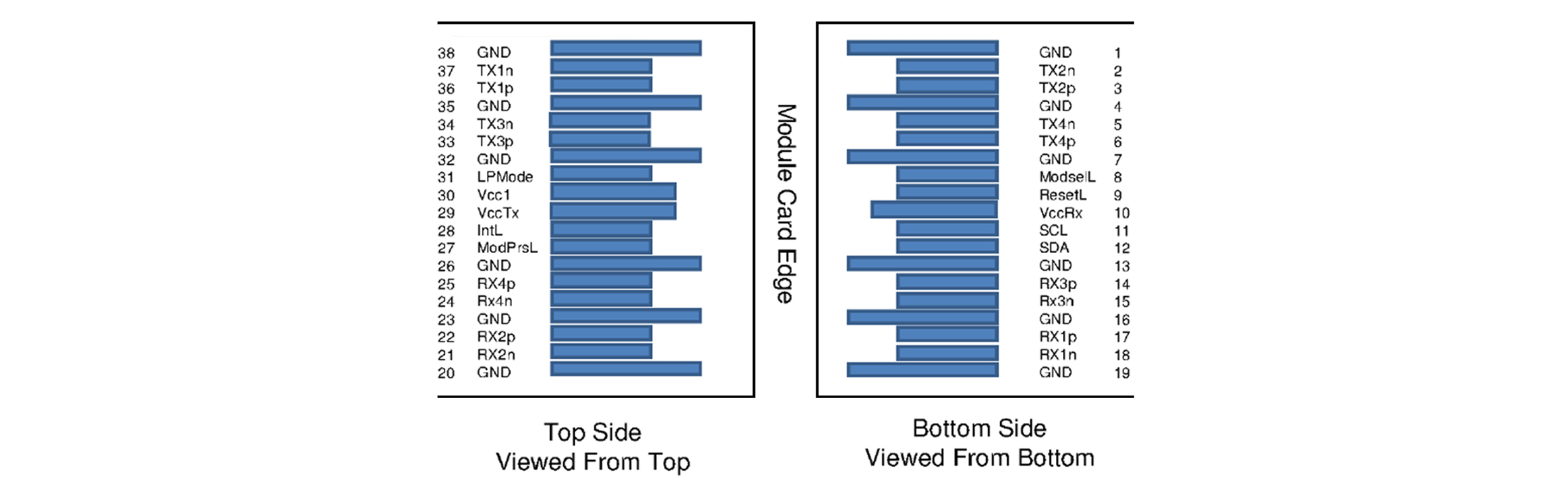
| Pin | Symbol | Name/Description | |||||||
| 1 | GND | Ground | |||||||
| 2 | Tx2n | Transmitter inverted data input | |||||||
| 3 | Tx2p | Transmitter non-inverted data input | |||||||
| 4 | GND | Ground | |||||||
| 5 | Tx4n | Transmitter inverted data input | |||||||
| 6 | Tx4p | Transmitter non-inverted data input | |||||||
| 7 | GND | Ground | |||||||
| 8 | ModSelL | Module select | |||||||
| 9 | ResetL | Module reset | |||||||
| 10 | VCCRx | +3.3V power supply receiver | |||||||
| 11 | SCL | 2-wire serial interface clock | |||||||
| 12 | SDA | 2-wire serial interface data | |||||||
| 13 | GND | Ground | |||||||
| 14 | Rx3p | Receiver non-inverted data output | |||||||
| 15 | Rx3n | Receiver inverted data output | |||||||
| 16 | GND | Ground | |||||||
| 17 | Rxlp | Receiver non-inverted data output | |||||||
| 18 | Rx1n | Receiver inverted data output | |||||||
| 19 | GND | Ground | |||||||
| 20 | GND | Ground | |||||||
| 21 | Rx2n | Receiver inverted data output | |||||||
| 22 | Rx2p | Receiver non-inverted data output | |||||||
| 23 | GND | Ground | |||||||
| 24 | Rx4n | Receiver inverted data output | |||||||
| 25 | Rx4p | Receiver non-inverted data output | |||||||
| 26 | GND | Ground | |||||||
| 27 | ModPrsL | Module present | |||||||
| 28 | IntL | Interrupt | |||||||
| 29 | VCC Tx | +3.3V power supply transmitter | |||||||
| 30 | VCC1 | +3.3V power Supply | |||||||
| 31 | LPMode | Low power mode | |||||||
| 32 | GND | Ground | |||||||
| 33 | Tx3p | Transmitter non-inverted data input | |||||||
| 34 | Tx3n | Transmitter inverted data input | |||||||
| 35 | GND | Ground | |||||||
| 36 | Txlp | Transmitter non-inverted dataInput | |||||||
| 37 | Tx1n | Transmitter inverted data input | |||||||
| 38 | GND | Ground | |||||||


 Wendy
Wendy Sophie
 Jeanne