


|
产品型号
|
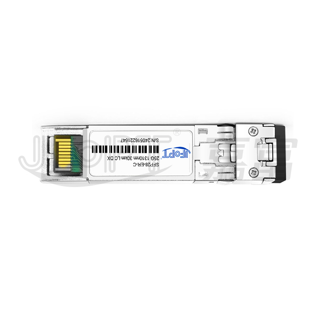
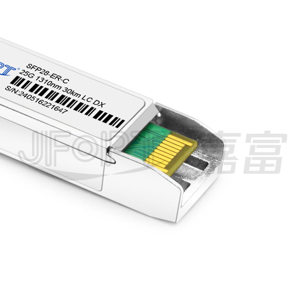
JFTSM-SFP28-25-13-30(ER)-LCD
|
工厂品牌
|
JFOPT嘉富
|
|
封装形式
|
SFP28
|
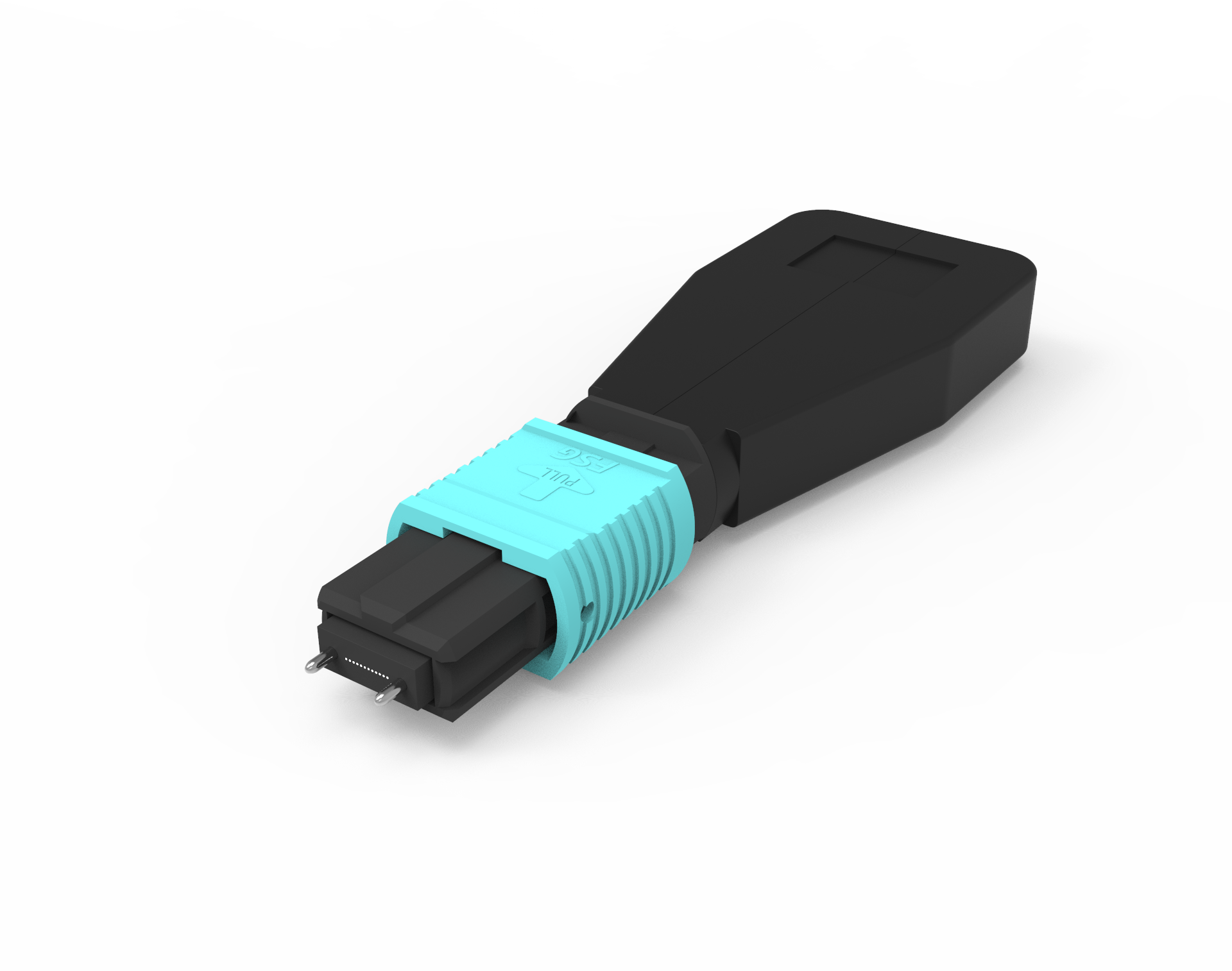
光口类型
|
双联LC
|
|
最高总速率
|
25.78G
|
每通道速率
|
10.31Gbps
|
|
最大传输距离
|
30km
|
||
|
工作波长
|
1310nm
|
工作电压
|
3.3V
|
|
光纤型号
|
SMF
|
纤芯尺寸
|
9/125
|
|
发射器类型
|
DML
|
接收器类型
|
APD
|
|
发射功率
|
-0.5~6.5dBm
|
接收灵敏度
|
<19.5dBm
|
|
数字诊断(DDM)
|
YES
|
接收过载
|
-5dBm
|
|
功耗
|
≤2W
|
支持协议
|
SFF-8472, SFF-8432, SFF-8431
|
|
工作温度(商业级)
|
0℃~+70℃
|
储存温度(商业级)
|
-40℃~+85℃
|
生产线介绍
PRODUCTION LINE INTRODUCTION
JFOPT嘉富持续投入光模块生产领域,产品覆盖1*9、SFP、10G、25G、100G、200G、400G、800G GPON/EPON/XG/XGSPON OLT等全系列光模块。同时为下游同行提供TOSA、ROSA、BOSA等光器件半成品解决方案。JFOPT嘉富生产线具备日产量一万只光模块、两万只光器件的能力。此外,JFOPT嘉富光模块拥有业界领先的耐高温、抗干扰特性,广泛应用于计算中心、运营商、交通安防、电力设施等行业领域。
产品介绍
PRODUCT PRESENTATION
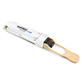
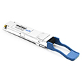
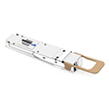
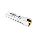
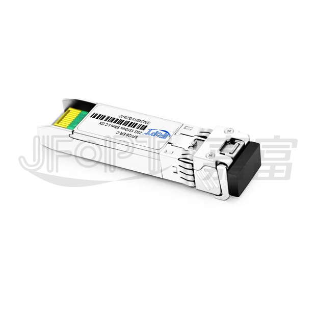
JFOPT SFP28 25G 1310nm 30km ER LC DX光模块专为以太网链路设计,支持最高25.78 Gb/s数据传输速率,在无需前向纠错(FEC)的情况下可实现长达30公里的传输距离。该模块符合SFF-8472标准,兼容SFF-8432及SFF-8431相关章节,同时依据2011/96/EU指令满足RoHS标准且无铅环保。
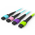
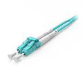
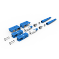
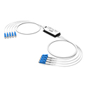
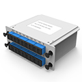
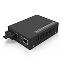
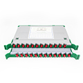
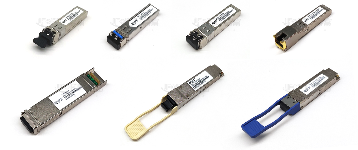
光模块系列产品
TRANSCEIVER SERIES PRODUCTS
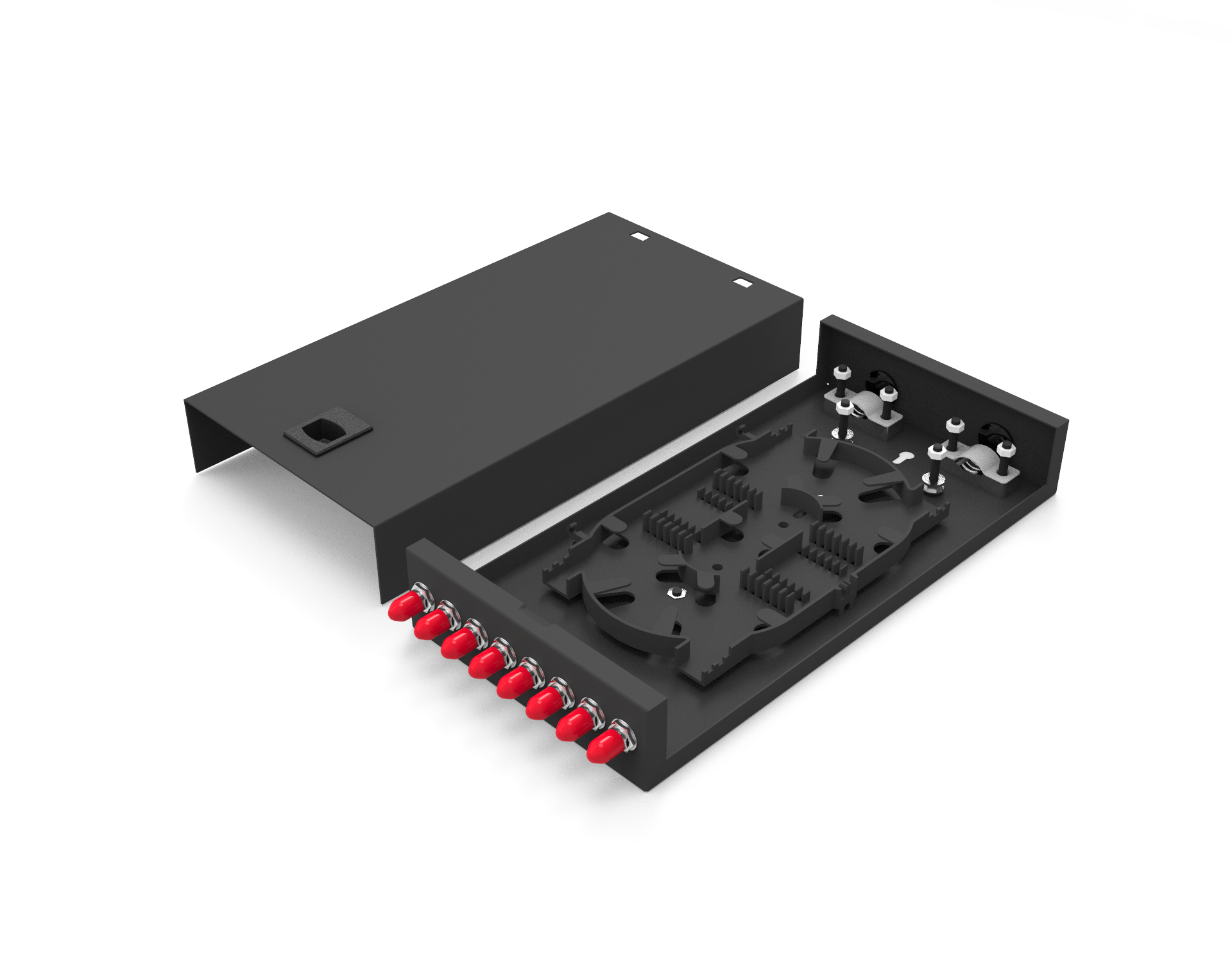
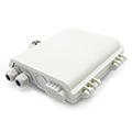
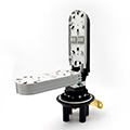
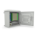
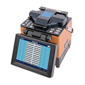
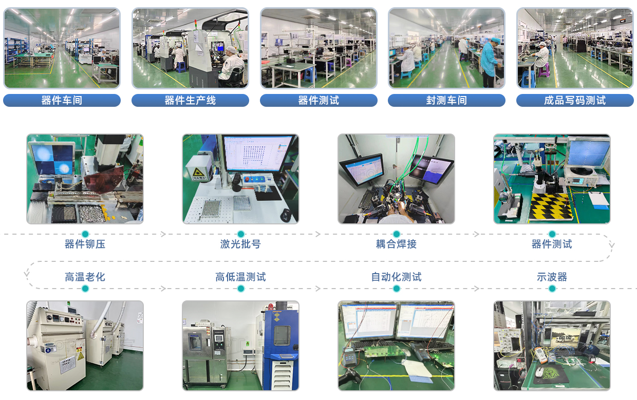
生产及检测设备
PRODUCTION & TESTING EQUIPMENT
产品特点
FEATURES
| UP to 25.78Gb/s data links | Hot-pluggable SFP28 footprint | ||||||||
| Duplex LC connector | DML laser transmitter, APD photo detector | ||||||||
| Up to 30km on SMF without FEC | Single 3.3V power supply | ||||||||
| Operating case temperature range: 0~ 70°C | 2-wire interface for management specifications compliant with SFF 8472 digital diagnostic monitoring interface for optical transceivers |
应用范围
APPLICATION
| High-speed storage area networks | CPRI 10 |
符合标准
STANDARD COMPLIANCE

绝对最大额定值
ABSOLUTE MAXIMUM RATINGS
| Parameter | Symbol | Min. | Typ. | Max. | Unit | ||||
| Storage temperature | TS | -40 | - | 85 | °C | ||||
| Case operating temperature | TA | 0 | - | 70 | °C | ||||
| Maximum supply voltage | Vcc | 0 | - | 3.6 | V | ||||
| Relative humidity | RH | 0 | - | 85 | % | ||||
电气特性
ELECTRICALCTRICAL CHARACTERISTICS
| Parameter | Symbol | Min. | Typ. | Max. | Unit | Note | |||
| Supply voltage | VCC | 3.15 | - | 3.46 | V | - | |||
| Supply current | Icc | - | - | 450 | mA | - | |||
| Power consumption | P | - | - | 1.5 | W | - | |||
| Data rate | R | - | 25.8 | - | Gb/s | - | |||
Transmitter |
|||||||||
| Input differential impedance | Rin | - | 100 | - | Ω | 1 | |||
| Differential input voltage swing | Vin,pp | 180 | - | 700 | mV | 2 | |||
| Transmit disable voltage | VD | 2 | - | Vcc | V | 3 | |||
| Transmit enable voltage | VEN | Vee | - | Vee+0.8 | V | - | |||
Receiver |
|||||||||
| Single ended output voltage tolerance |
V | -0.3 | - | 4 | V | - | |||
| Rx output diff voltage | Vo | 185 | - | 800 | mV | - | |||
| LOS fault | VLOS fault | 2 | - | VccHOST | V | 4 | |||
| LOS normal | VLOS norm | Vee | - | Vee+0.8 | V | 4 | |||
| Notes: 1.Connected directly to TX data input pins. AC coupling from pins into laser driver IC. 2.Per SFF-8431 Rev 3.0 3.Into 100 ohms differential termination. 4.LOS is an open collector output. Should be pulled up with 4.7k – 10kΩ on the host board. Normal operation is logic 0; loss of signal is logic 1. Maximum pull-up voltage is 5.5V. |
|||||||||
光学特性
OPTICAL CHARACTERISTICS
| Parameter | Symbol | Min. | Typ. | Max | Unit | Notes | |||
Transmitter |
|||||||||
| Center wavelength | λt | 1295 | - | 1325 | nm | - | |||
| Spectral width | △λ | - | - | 1 | nm | - | |||
| Average optical power | Pavg | 0 | - | +6 | dBm | 1 | |||
| Laser off power | Poff | - | - | -30 | dBm | - | |||
| Side mode suppression ratio | - | 30 | - | - | - | - | |||
| Extinction ratio | ER | 4 | - | - | dB | - | |||
| Optical return loss tolerance | - | - | - | -12 | dB | - | |||
Receiver |
|||||||||
| Center wavelength | λr | 1260 | - | 1370 | nm | - | |||
| Receiver sensitivity | Sen | - | - | -19 | dBm | 2 | |||
| Los assert | LOSA | -30 | - | dBm | - | ||||
| Los dessert | LOSD | - | - | -19 | dBm | - | |||
| Los hysteresis | LOSH | 0.5 | - | dB | - | ||||
| Overload | - | -6 | - | - | dBm | - | |||
Notes: 1.Average power figures are informative only, per IEEE802.3CC. 2.Receiver sensitivity is informative. Shall be measured with conformance test signal for . BER =5x 10⁻⁵. |
|||||||||
时序特性
TIMING CHARACTERISTICS
| Parameter | Symbol | Min. | Typ. | Max. | Unit | ||||
| TX_disable assert time | t_off | - | - | 100 | us | ||||
| TX_disable negate time | t_on | - | - | 2 | ms | ||||
| Time to initialize 2-wire interface | t_2w_start_up | - | - | 300 | ms | ||||
| Time to initialize | t_start_up | - | - | 300 | ms | ||||
| Time to initialize cooled module and time to power up a cooled module to power level II | t_start_up_cooled | - | - | 90 | s | ||||
| Time to power up to level II | t_power_level2 | - | - | 300 | ms | ||||
| Time to power down from level II | t_power_down | - | - | 300 | ms | ||||
| Tx_fault assert | Tx_Fault_on | - | - | 1 | ms | ||||
| Tx_fault assert for cooled module | Tx_Fault_on_cooled | - | - | 50 | ms | ||||
| TX_FAULT reset | t_reset | 10 | - | - | us | ||||
| Rx_LOS assert delay | t_los_on | - | - | 100 | us | ||||
| Rx_LOS negate delay | t_los_off | - | - | 100 | us | ||||
数字诊断规格
DIGITAL DIAGNOSTIC SPECIFICATIONS
| Parameter | Symbol | Min. | Max. | Accuracy | Unit | ||||
| Transceiver temperature | T | 0 | +70 | ±3.0°C | °C | ||||
| Transceiver supply voltage | DDVoltage | 3.15 | 3.45 | ±3% | V | ||||
| Transmitter bias current | DDBias | 0 | 35 | ±10% | mA | ||||
| Transmitter output power | DDTx-Power | -5 | +5 | ±2dB | dBm | ||||
| Receiver average optical input power | DDRx-Power | -16 | -3 | ±2dB | dBm | ||||
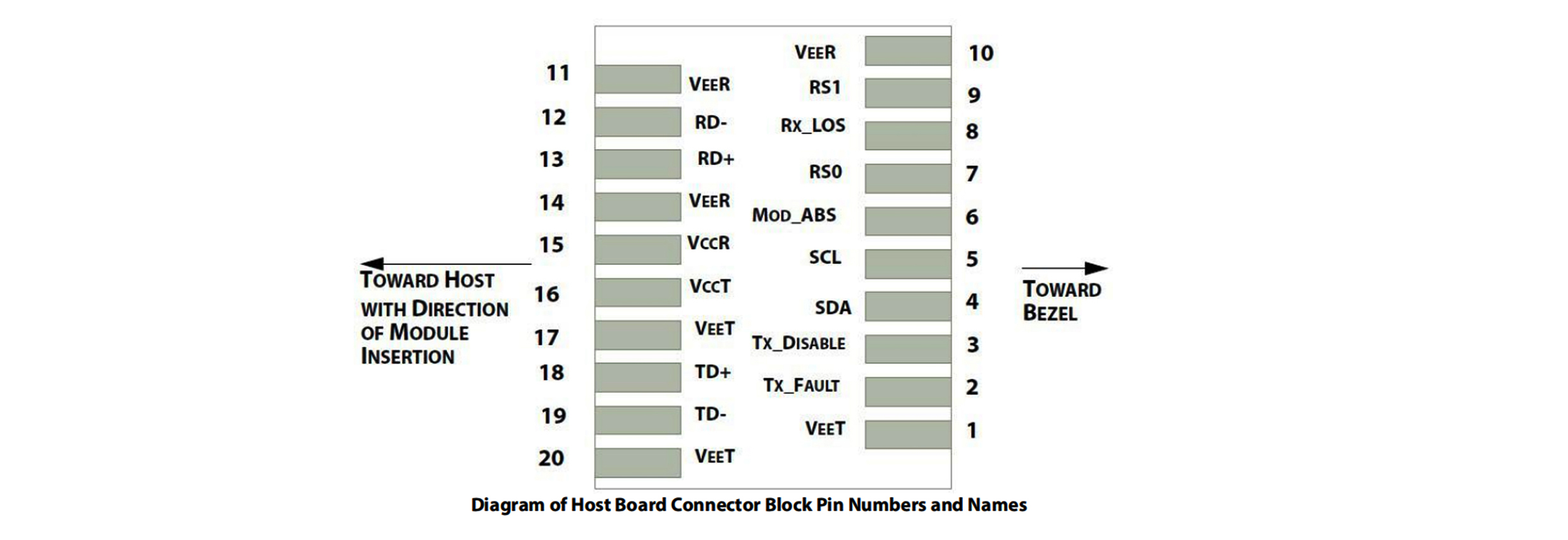
引脚描述
PIN DESCRIPTION
| Pin | Symbol | Name/Description | Plug Seq. | ||||||
| 1 | VeeT | Module transmitter ground | 1 | ||||||
| 2 | TX fault | Module transmitter fault | 2 | ||||||
| 3 | TX disable | Transmitter disable; turns off transmitter laser output | 3 | ||||||
| 4 | SDL | 2 wire serial interface data input/output (SDA) | 4 | ||||||
| 5 | SCL | 2 wire serial interface clock input (SCL) | 4 | ||||||
| 6 | MOD_ABS | Module absent, connect to VeeR or VeeT in the module | 2 | ||||||
| 7 | RS0 | Rate select0: module inputs and are pulled low to VeeT with >30 kΩ resistorsin the module. | - | ||||||
| 8 | LOS | Receiver Loss of signal indication | - | ||||||
| 9 | RS1 | Rate select1: module inputs and are pulled low to VeeT with >30 kΩ resistorsin the module. | - | ||||||
| 10 | VeeR | Module receiver ground | 1 | ||||||
| 11 | VeeR | Module receiver ground | 1 | ||||||
| 12 | RD- | Receiver inverted data out put | - | ||||||
| 13 | RD+ | Receiver non-inverted data out put | - | ||||||
| 14 | VeeR | Module receiver ground | 1 | ||||||
| 15 | VccR | Module receiver 3.3V supply | - | ||||||
| 16 | VccT | Module transmitter 3.3V supply | - | ||||||
| 17 | VeeT | Module transmitter ground | 1 | ||||||
| 18 | TD+ | Transmitter non-inverted data out put | - | ||||||
| 19 | TD- | Transmitter inverted data out put | - | ||||||
| 20 | VeeT | Module transmitter ground | 1 | ||||||
| Notes: 1.The module ground pins shall be isolated from the module case. 2.This pin is an open collector/drain output pin and shall be pulled up with 4.7K-10Kohms to Host_Vcc on the host board. 3.This pin shall be pulled up with 4.7K-10Kohms to VccT in the module. 4.This pin is an open collector/drain output pin and shall be pulled up with 4.7K-10Kohms to Host_Vcc on the host board. |
|||||||||
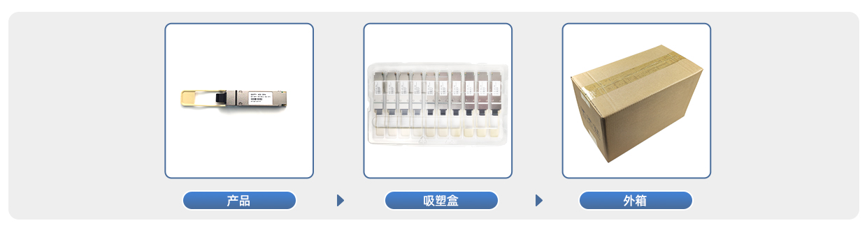
产品包装
PRODUCT PACKAGING
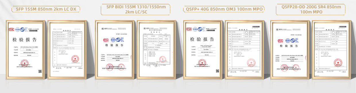
产品认证
PRODUCT CERTIFICATION
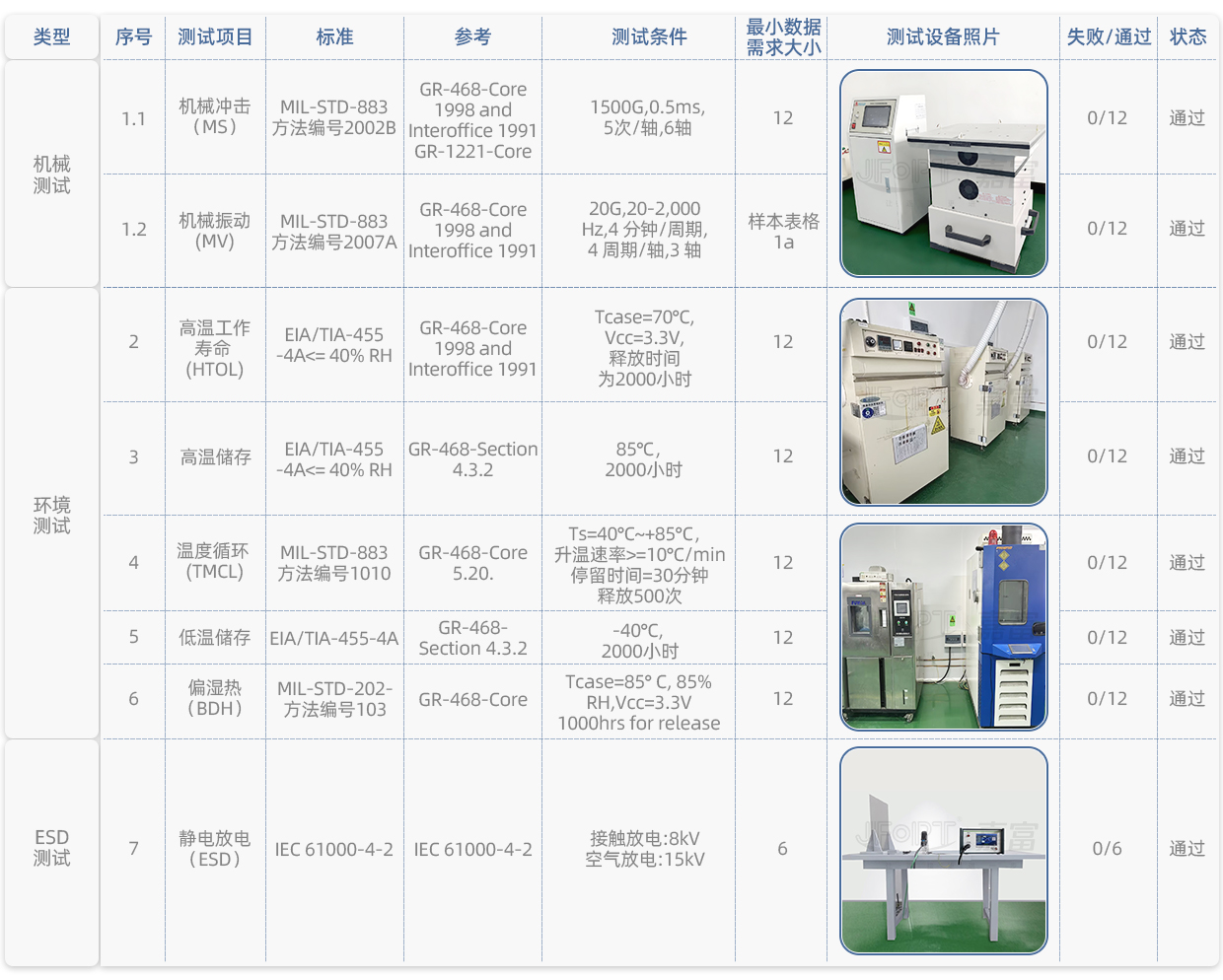
质量优势
QUALITY ADVANTAGE
兼容品牌
COMPATIBLE BRANDS


 Wendy
Wendy Sophie
 Jeanne